


CLOCK GENERATION AND POWER MANAGEMENT
5-12
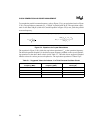
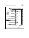
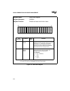
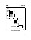
Figure 5-9. Power-Save Register
Register Name: Power Save Register
Register Mnemonic: PWRSAV
Register Function: Enables and sets clock division factor.
Bit
Mnemonic
Bit Name
Reset
State
Function
PSEN Power Save
Enable
0H Setting this bit enables Power Save mode and
divides the internal operating clock by the value
defined by F1:0. Clearing this bit disables
Power-Save mode and forces the CPU to
operate at full speed. PSEN is automatically
cleared whenever an interrupt occurs.
F1:0 Clock
Division
Factor
0H These bits control the clock division factor used
when Power Save mode is enabled. The
allowable values are listed below:
F1 F0 Divisor
0 0 By 1 (undivided)
01By 4
10By 8
11By 16
NOTE: Reserved register bits are shown with gray shading. Reserved bits must be written
to a logic zero to ensure compatibility with future Intel products.
A1130-0A
15 0
F
1
F
0
P
S
E
N