


BUS INTERFACE UNIT
3-40
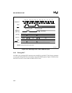
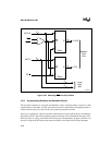
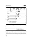
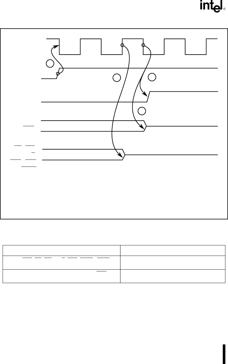
Figure 3-34. Timing Sequence Entering HOLD
3.7.1.1 HOLD Bus Latency
The duration between the time that the external device asserts HOLD and the time that the BIU
asserts HLDA is known as bus latency. In Figure 3-34, the two-clock delay between HOLD and
HLDA represents the shortest bus latency. Normally this occurs only if the bus is idle or halted
or if the bus hold request occurs just before the BIU begins another bus cycle.
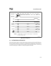
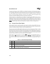
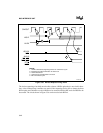
Table 3-8. Signal Condition Entering HOLD
Signal HOLD Condition
A19:16, S2:0
, RD, WR, DT/R, BHE (RFSH), LOCK These signals float one-half clock before HLDA
is generated (i.e., phase 2).
AD15:0 (16-bit), AD7:0 (8-bit), A15:8 (8-bit), DEN
These signals float during the same clock in
which HLDA is generated (i.e., phase 1).
A1518-0A
HLDA
CLKOUT
HOLD
NOTES:
1. T
HVCL
: HOLD input to clock low
2. T
CHCZ
: Clock high to output float
3. T
CLAZ
: Clock low to output float
4. T
CLHAV
: Clock low to HLDA high
1
4
2
3
Float
Float
AD15:0
DEN
A19:16
RD, WR,
DT/R,
BHE, S2:0
LOCK