


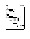

CHIP-SELECT UNIT
6-6
6.4 PROGRAMMING
Four registers determine the operating characteristics of the chip-selects. The Peripheral Control
Block defines the location of the Chip-Select Unit registers. Table 6-1 lists the registers and their
associated programming names.
The control registers (Figures 6-5 through 6-7) define the base address and bus ready and wait
state requirements for the corresponding chip-selects. The alternate control register (Figure 6-9)
defines the block size for MCS3:0
. It also selects memory or I/O space for PCS6:0, selects the
function of the PCS6:5
pins, and defines the bus ready and wait state requirements for PCS6:4.
6.4.1 Initialization Sequence
Chip-selects do not have to be initialized in any specific order. However, the following guidelines
help prevent a system failure.
1. Initialize local memory chip-selects
2. Initialize local peripheral chip-selects
3. Perform local diagnostics
4. Initialize off-board memory and peripheral chip-selects
5. Complete system diagnostics
An unmasked interrupt or NMI must not occur until the interrupt vector addresses have been writ-
ten to memory. Failure to prevent an interrupt from occurring during initialization will cause a
system failure. Use external logic to generate the chip-select if interrupts cannot be masked prior
to initialization.
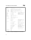
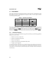
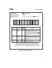
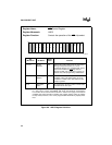
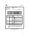
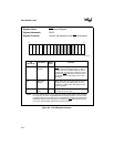
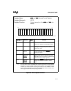
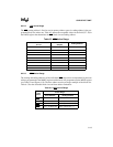
Table 6-1. Chip-Select Unit Registers
Control Register
Mnemonic
Alternate Register
Mnemonic
Chip-Select Affected
UMCS None UCS
LMCS None LCS
MMCS MPCS MCS3:0
PACS MPCS PCS6:0