


BUS INTERFACE UNIT
3-2
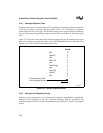
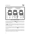
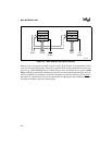
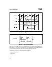
Figure 3-1. Physical Data Bus Models
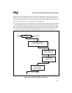
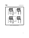
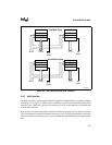
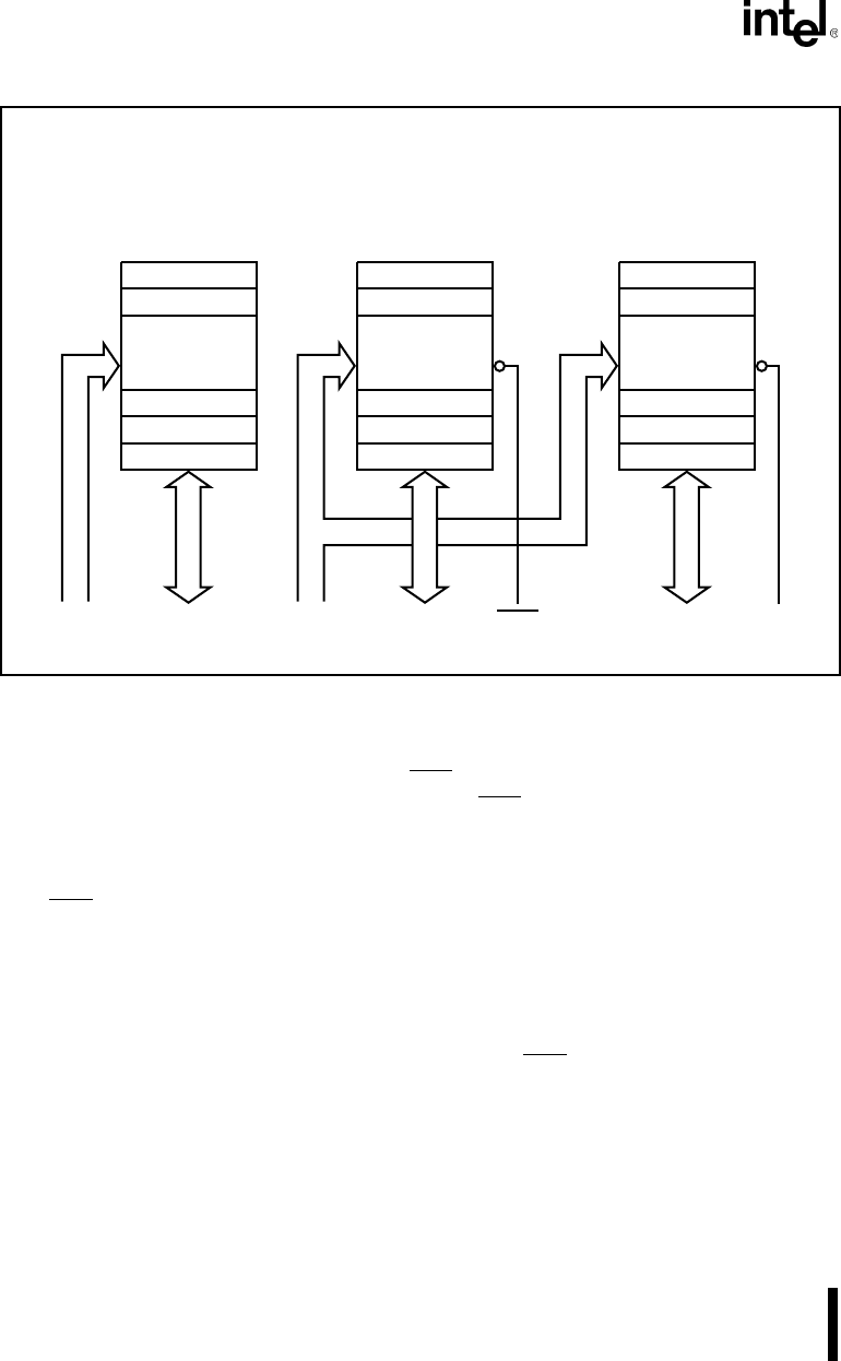
Byte transfers to even addresses transfer information over the lower half of the data bus (see Fig-
ure 3-2). A0 low enables the lower bank, while BHE
high disables the upper bank. The data value
from the upper bank is ignored during a bus read cycle. BHE
high prevents a write operation from
destroying data in the upper bank.
Byte transfers to odd addresses transfer information over the upper half of the data bus (see Figure
3-2). BHE
low enables the upper bank, while A0 high disables the lower bank. The data value
from the lower bank is ignored during a bus read cycle. A0 high prevents a write operation from
destroying data in the lower bank.
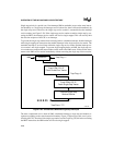
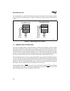
To access even-addressed 16-bit words (two consecutive bytes with the least-significant byte at
an even address), information is transferred over both halves of the data bus (see Figure 3-3).
A19:1 select the appropriate byte within each bank. A0 and BHE
drive low to enable both banks
simultaneously.
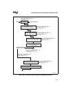
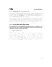
Odd-addressed word accesses require the BIU to split the transfer into two byte operations (see
Figure 3-4). The first operation transfers data over the upper half of the bus, while the second op-
eration transfers data over the lower half of the bus. The BIU automatically executes the two-byte
sequence whenever an odd-addressed word access is performed.
0
2
4
FFFFC
FFFFE
FFFFF
FFFFD
1
3
5
512 KBytes
512 KBytes
1 MByte
Physical Implementation
of the Address Space for
16-Bit Systems
Physical Implementation
of the Address Space for
8-Bit Systems
D7:0 D15:8A19:1A19:0 D7:0
BHE A0
FFFFF
FFFFE
0
1
2
A1100-0A