


6-11
CHIP-SELECT UNIT
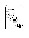
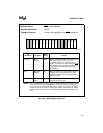
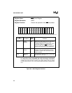
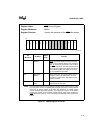
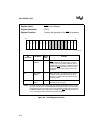
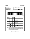
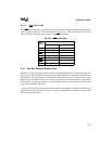
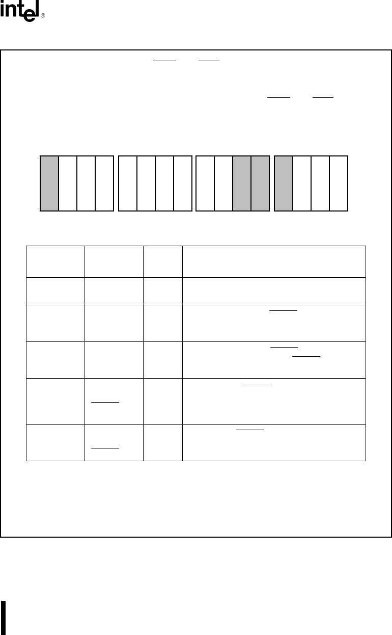
Figure 6-9. MPCS Register Definition
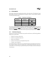
Register Name: MCS and PCS Alternate Control Register
Register Mnemonic: MPCS
Register Function: Controls operation of the MCS
and PCS chip-
selects.
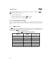
Bit
Mnemonic
Bit Name
Reset
State
Function
M6:0 Block Size XXH Defines the block size for the MCS chip-selects.
Table 6-5 on page 6-14 lists allowable values.
EX Pin Selector XH Setting EX configures PCS6:5
as chip-selects.
Clearing EX configures the pins as latched
address bits A2:A1.
MS Bus Cycle
Selector
XH Clearing MS activates PCS6:0
for I/O bus
cycles. Setting MS activates PCS6:0
for
memory bus cycles.
R2 Bus Ready
Disable for
PCS6:4
X Applies only to PCS6:4. When R2 is clear, bus
ready must be active to complete a bus cycle.
When R2 is set, R1:0 control the number of bus
wait states and bus ready is ignored.
R1:0 Wait State
Value for
PCS6:4
3H Apply only to PCS6:4. R1:0 define the minimum
number of wait states inserted into the bus
cycle.
NOTE: Reserved register bits are shown with gray shading. Reserved bits must be written
to a logic zero to ensure compatibility with future Intel products. A starting address
other than an integer multiple of the block size defined in this register causes
unreliable chip-select operation. Reading this register and the MMCS or PACS
register (before writing them) enables the associated chip-selects; however, none
of the programmable fields will be properly initialized.
15 0
R
1
R
0
R
2
E
X
M
S
M
1
M
0
M
3
M
2
M
5
M
4
M
6
A1144-0A