


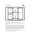

INTERRUPT CONTROL UNIT
8-12
8.4.1 Interrupt Control Registers
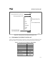
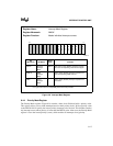
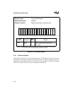
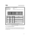
Each interrupt source has its own Interrupt Control register. The Interrupt Control register allows
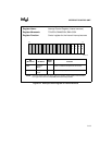
you to define the behavior of each interrupt source. Figure 8-4 shows the registers for the timers
and DMA channels, Figure 8-5 shows the registers for INT3:2, and Figure 8-6 shows the registers
for INT0 and INT1.
All Interrupt Control registers have a three-bit field (PM2:0) that defines the priority level for the
interrupt source and a mask bit (MSK) that enables or disables the interrupt source. The mask bit
is the same as the one in the Interrupt Mask register. Modifying a bit in either register also mod-
ifies that same bit in the other register.
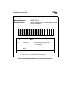
The Interrupt Control registers for the external interrupt pins also have a bit (LVL) that selects
level-triggered or edge-triggered mode for that interrupt. (See “Edge and Level Triggering” on
page 8-10.)
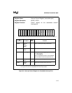
The Interrupt Control registers for the cascadable external interrupt pins (INT0 and INT1) have
two additional bits to support the external 8259As. The CAS bit enables cascade mode, and the
SFNM bit enables special fully nested mode.
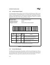
In-Service 2CH
Priority Mask 2AH
Interrupt Mask 28H
Poll Status 26H
Poll 24H
EOI 22H
Table 8-3. Interrupt Control Unit Registers in Master Mode (Continued)
Register Name Offset Address