


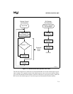

REFRESH CONTROL UNIT
7-6
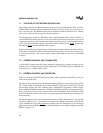
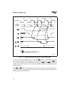
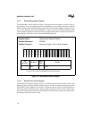
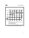
Figure 7-4. Suggested DRAM Control Signal Timing Relationships
The cycle begins with presentation of the row address. RAS should go active on the falling edge
of T2. At the rising edge of T2, the address lines should switch to a column address. CAS
goes
active on the falling edge of T3. Refresh cycles do not require CAS
. When CAS is present, the
“dummy read” cycle becomes a true read cycle (the DRAM drives the bus), and the DRAM row
still gets refreshed.
Both RAS
and CAS stay active during any wait states. They go inactive on the falling edge of T4.
At the rising edge of T4, the address multiplexer shifts to its original selection (row addressing),
preparing for the next DRAM access.
S2:0
CLKOUT
Muxed
Address
NOTES:
1. CAS is unnecessary for refresh cycles only.
2. WE is necessary for write cycles only.
CS
RAS
CAS
WE
T4 T1 T2 T3/TW T4
1
2
Row
Column
A1267-0A