


signal as the signal is clocked at 8 MHz on both the backplane and the
transmission media (lobe cables and inter-wiring closet cables).
8.3 Dual Phase Lock Loop
The intent of the dual PLL design of the 8260 is to isolate lobes from each other
so the lobe length or type of cable will not affect what can be achieved on any
other lobe of a ring segment. Below is a summary of the Dual PLL concept and
its implementation in the 8260.
The current IBM token-ring adapters use a Phase Lock Loop (PLL) to derive a
clock signal from the incoming data signal, and then use that clock to retransmit
the data. As data is affected by crosstalk, noise, cable characteristics, etc. the
phase of the transitions in the data shift around. This is referred to as jitter.
Most of this jitter is filtered out by re-clocking the signal, but to the degree that
the jitter affects the PLL, and therefore the clock output of the PLL, that jitter is
passed on by the adapter. This jitter in the clock signal is passed on to the next
station downstream. With each additional adapter, the amount of shift in the
transitions grows. Eventually, the shift is large enough and fast enough that the
next PLL cannot track with it, so the signal fails to be accurately retransmitted.
PLLs have a characteristic associated with them called
bandwidth
. The
bandwidth determines how fast a change the PLL can track. The larger the
bandwidth, the better the PLL can track the fast changing incoming signals, but
higher bandwidths also mean more of the jitter is passed to the output, so just
increasing the bandwidth does not result in more stations on a ring. What is
needed is a PLL that behaves like a
wideband
PLL, but the clock output should
behave like that from a PLL with a narrow bandwidth. That is what is
implemented with the dual PLL concept.
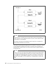
A signal coming into an active port on an 8260 is first received by a PLL with a
wideband characteristic. This bandwidth is set at approximately 400 kHz -
similar to the PLL on the current IBM token-ring adapters. The clocked data
from the wideband PLL receiver is then fed through a buffer, into a PLL circuit
with a
narrowband
characteristic. As a comparison, the bandwidth of this PLL is
set around 50 kHz. The buffer in between is required because at any point in
time the wideband PLL may be clocking the incoming data at a different rate
than the narrowband PLL is clocking data going out (because the wideband PLL
shifts faster than the narrowband PLL). The result is a circuit that can receive a
signal with a fair amount of jitter, but it retransmits a signal with a significant
reduction in jitter.
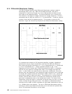
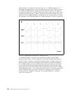
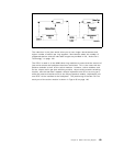
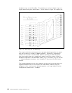
As far as practical implementation, the 8260 puts a wideband PLL receiver on
the incoming signal from each lobe, and puts the narrowband PLL in the
transmitter of each lobe output. Figure 84 on page 139 shows the components
of the DPLL as implemented in the 8260 media modules.
138 8260 Multiprotocol Intelligent Switching Hub