


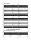
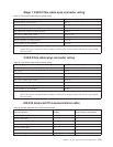
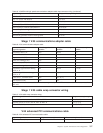
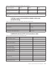

Table 65. V.36/EIA 449 high speed communications adapter cable wrap connector wiring (continued)
Signal designation Wrap connector pin to pin
DTRBtoDSRB 30to29
RTS A to CTS A and RLSD A 7 to 9,13
RTS B to CTS B and RLSD B 25 to 27,31
TSET A (DTE) to TSET A (DCE) RSET A 17 to 5,8
TSET B (DTE) to TSET B (DCE) RSET B 35 to 23,26
Remote loopback to ring indicate 14 to 15
Local loopback to test indicate 10 to 18
Send circuit ground to receive circuit ground 37 to 20
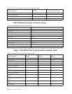
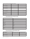
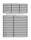
Stage 1 V.35 communications adapter cable
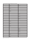
Table 66. V.35 communications adapter cable
Signal designation
Interchange circuit
number
Adapter connector pin
number
DCE connector pin
number
Transmitted data A, B 103 42, 26 P, S
Received data A, B 104 44, 31 R, T
Request to send (RTS) 105 4 C
Ready for sending (CTS) 106 5 D
Data set ready (DSR) 107 6 E
Received line signal (carrier) detector 109 8 F
Transmitter signal element timing
(DCE) A, B
114 48, 30 Y, A (A)
Receiver signal element timing
(DCE) A, B
115 13, 46 V, X
Cable ID 2, 1, common return 102 (17, 16, 7) B
Data terminal ready 108 24 H
Note: Cable ID 2, 1 is connected to common return pin 7 only at the DTE connector end and is not connected at the
DCE end.
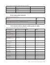
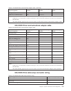
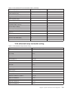
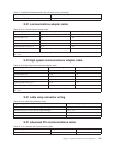
Stage 1 V.35 cable wrap connector wiring
Table 67. V.35 cable wrap connector wiring
Signal designation Wrap connector pin to pin
Transmit data A to receive data A, TSET A, RSET A P to (R, Y, V)
Transmit data B to receive data B, TSET B, RSET B S to (T, A, X)
RTS to CTS, DSR, carrier detector C to (D, E, F)
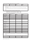
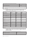
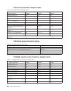
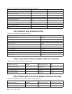
V.24 advanced PCI communications cable
Table 68. V.24 advanced PCI communications cable
Signal designation Adapter connector pin number DCE connector pin number
Transmitted data (TD) 13 2
Chapter 9. System Architecture and Configuration 257