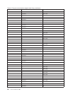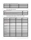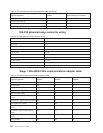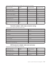
Table 68. V.24 advanced PCI communications cable (continued)
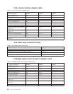
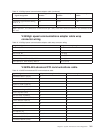
Signal designation Adapter connector pin number DCE connector pin number
Received data (RD) 6 3
Request to send (RTS) 2 4
Ready for sending (CTS) 33 5
Data set ready (DSR) 15 6
Signal Ground (SGND) 7,27 7
Received line signal (carrier) detector
(CD)
20 8
Transmitter Clock (TCLK) 29 15
Receiver Clock (RCLK) 26 17
Local Loop Back (LLB) 21 18
Data terminal ready (DTR) 4 20
Ring Indicate (RI) 31 22
Remote Loop Back (RLB) 23 21
Test Indicate (TI) 18 25
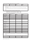
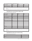
V.24 advanced wrap connector wiring
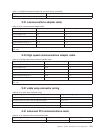
Table 69. V.24 advanced wrap connector wiring
Signal destination Wrap connector pin to pin
TD to RD 2 to 3
RD to TD 3 to 2
RTS to CTS, TCLK 4 to 5,15
CTS to RTS 5 to 4
DSR to DTR 6 to 20
CD to RLB 8 to 21
TCLK to RTS 15 to 4
RCLK to DTR 17 to 20
LLB to TI 18 to 25
DTR to DSR, RCLK 20 to 6,17
RLB to CD, RI 21 to 8,22
RI to RLB 22 to 21
TI to LLB 25 to 18
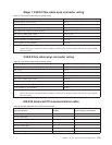
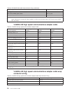
V.35 advanced PCI communications cable
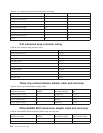
Table 70. V.35 advanced PCI communications cable
Signal designation Adapter connector pin number DCE connector pin number
Transmitter Clock B (TCLK-B) 28 AA
Signal Ground (SGND) 7,8,27 B
Request to send (RTS) 2 C
Ready for sending (CTS) 33 D
258 Service Functions V5R2


