


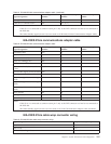
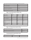
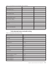
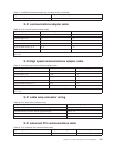

Table 70. V.35 advanced PCI communications cable (continued)
Signal designation Adapter connector pin number DCE connector pin number
Data set ready (DSR) 15 E
Carrier detector (CD) 20 F
Data terminal ready (DTR) 4 H
Ring Indicate (RI) 31 J
Local Loop Back (LLB) 21 L
Remote Loop Back (RLB) 23 N
Test Indicate (TI) 18 NN
Transmitted Data A (TD-A) 13 P
Received data A (RD-A) 6 R
Transmitted Data B (TD-B) 12 S
Received Data B (RD-B) 5 T
DTECK A 36 U
Receiver Clock A (RCLK-A) 26 V
DTECK B 35 W
Receiver Clock B (RCLK-B) 25 X
Transmitter Clock A (TCLK-A) 29 Y
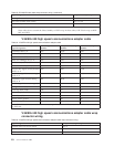
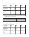
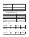
V.35 advanced wrap connector wiring
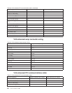
Table 71. V.35 advanced wrap connector wiring
Signal destination Wrap connector pin to pin
TCLK-B to DTECK-B AA to W
RTStoCTS CtoD
CTS to RTS D to C
DSR to DTR E to H
CD to DTR F to H
DTR to DSR, CD H to E,F
RI to RLB J to N
LLB to TI L to NN
RLB to RI N to J
TI to LLB NN to L
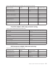
TD-A to RD-A P to R
RD-A to TD-A R to P
TD-B to RD-B S to T
RD-B to TD-B T to S
DTECK-A to RCLK-A, TCLK-A U to V,Y
RCLK-A to DTECK-A V to U
DTECK-B to TCLK-B, RCLK-B W to AA,X
RCLK-B to DTECK-B X to W
TCLK-A to DTECK-A Y to U
Chapter 9. System Architecture and Configuration 259