xContents
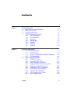
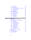
6.3 AC Characteristics 6-9
6.4 PCI and External Memory Interface Timing Diagrams 6-11
6.4.1 Target Timing 6-13
6.4.2 Initiator Timing 6-19
6.4.3 External Memory Timing 6-35
6.5 SCSI Timing Diagrams 6-52
6.6 Package Diagrams 6-58
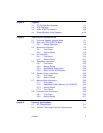
Appendix A Register Summary
Appendix B External Memory Interface Diagram Examples
Index
Customer Feedback
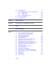
Figures
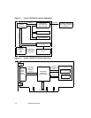
1.1 Typical LSI53C875A System Application 1-2
1.2 Typical LSI53C875A Board Application 1-2
2.1 LSI53C875A Block Diagram 2-2
2.2 Parity Checking/Generation 2-27
2.3 DMA FIFO Sections 2-28
2.4 LSI53C875A Host Interface SCSI Data Paths 2-29
2.5 Regulated Termination for Ultra SCSI 2-33
2.6 Determining the Synchronous Transfer Rate 2-35
2.7 Block Move and Chained Block Move Instructions 2-45
3.1 LSI53C875A Functional Signal Grouping 3-2
5.1 SCRIPTS Overview 5-5
6.1 Rise and Fall Time Test Condition 6-7
6.2 SCSI Input Filtering 6-7
6.3 Hysteresis of SCSI Receivers 6-7
6.4 Input Current as a Function of Input Voltage 6-8
6.5 Output Current as a Function of Output Voltage 6-8
6.6 External Clock 6-9
6.7 Reset Input 6-10
6.8 Interrupt Output 6-11


