64-Bit SCRIPTS Selectors 4-99
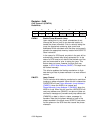
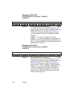
Register: 0x5A–0x5B
Reserved
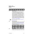
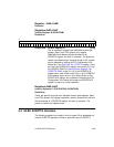
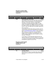
Registers:0x5C–0x5F
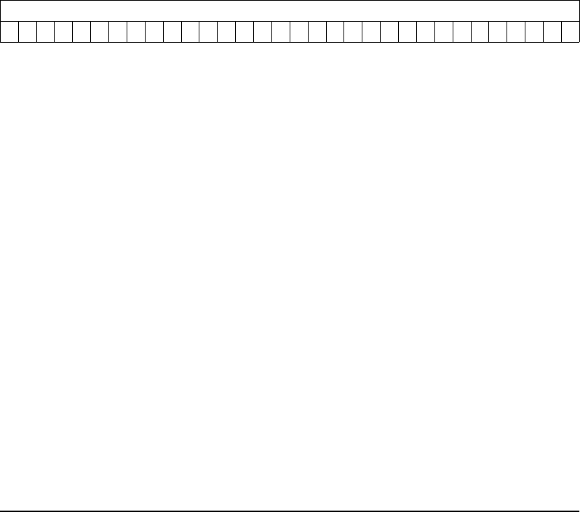
Scratch Register B (SCRATCHB)
Read/Write
SCRATCHB Scratch Register B [31:0]
This is a general purpose user definable scratch pad
register. Apart from CPU access, only register
Read/Write and Memory Moves directed at the
SCRATCH register will alter its contents. The power-up
values are indeterminate. A special mode of this register
can be enabled by setting the PCI Configuration Into
Enable bit in the C hip Tes t Two (C TEST2) register. If this
bit is set, the SCRATCH B register returns bits [31:12] of
the SCRIPTS RAM PCI Base Address Register Two
(SCRIPTS RAM) in bits [31:12] of the SCRATCH B
register when read. When read, bits [11:0] of SCRATCH
B will always return zeros in this mode. Writes to the
SCRATCH B register are unaffected. Resetting the PCI
Configuration Into Enable bit causes the SCRATCH B
register to return to normal operation.
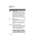
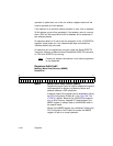
Registers:0x60–0x9F
Scratch Registers C–R (SCRATCHC–SCRATCHR)
Read/Write
These are general purpose user definable scratch pad registers. Apart
from CPU access, only register read/write, memory moves and Load and
Stores directed at a SCRATCH register will alter its contents. The
power-up values are indeterminate.
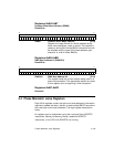
4.3 64-Bit SCRIPTS Selectors
The following registers are used to hold the upper 32-bit addresses for
various SCRIPTS operations. When a particular type of SCRIPTS
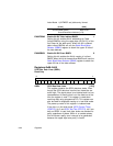
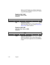
31 0
SCRATCHB
xxxxxxxxxxxxxxxxxxxxxxxxxxxxxxxx


