


3-12 Signal Descriptions
3.7 Test Interface Signals
Table 3.1 3 describes Test Interface signals.
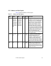
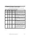
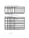
MAD[7:0] 59–62,
64–67
L7, M7,
N7, K7,
M8, N8,
L8, K8
I/O 4 mA Memory Address/Data Bus. This bus is used in
conjunction with the memory address strobe pins
and external address latches to assemble up to a
20-bit address for an external EEPROM or flash
memory. This bus will put out the least significant
byte first and finishes with the most significant bits.
It is also used to write data to a flash memory or
read data into the chip from external EEPROM/
flash memory. These pins have static pull-downs.
Table 3.12 ROM Flash and Memory Interface Signals (Cont.)
Name PQFP BGA Type Strength Description
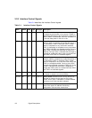
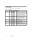
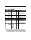
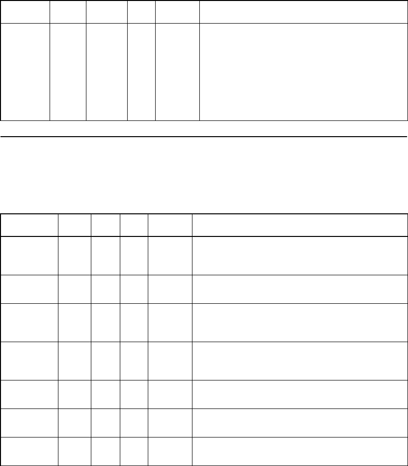
Table 3.13 Test Interface Signals
Name PQFP BGA Type Strength Description
TEST_HSC/ 126 A11 I N/A Test Halt SCSI Clock. For LSI Logic test purposes
only. Pulled HIGH internally. This signal can also
cause a full chip reset.
TCK 130 A10 I N/A Test Clock. This pin provides the clock for the JTAG
test logic.
TMS 57 N6 I N/A Test Mode Select. The signal received at TMS is
decoded by the TAP controller to control JTAG test
operations. This pin has a static pull-down.
TDI 142 D7 I N/A Test Data In. Serial test instructions are received by
the JTAG test logic at this pin. This pin has a static
pull-down.
TEST_RST/ 127 C10 I N/A Test Reset. For test purposes only. Pulled HIGH
internally.
TDO 58 J6 O 4 mA Test Data Out. This pin is the serial output for test
instructions and data from the JTAG test logic.
TRST/ 131 C9 I N/A Test Reset. This pin provides a reset for JTAG Test
Logic. Pulled HIGH internally.