4-4 Registers
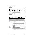
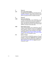
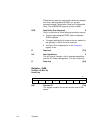
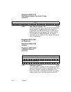
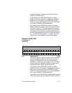
R Reserved 5
WIE Write and Invalidate Enable 4
This bit allows the LSI53C875A to generate write and
invalidate commands on the PCI bus. The WIE bit in the
DMA Control (DCNTL) register must also be set for the
device to generate Write and Invalidate commands.
R Reserved 3
EBM Enable Bus Mastering 2
This bit controls the ability of the LSI53C875A to act as
a master on the PCI bus. A value of zero disables this
device from generating PCI bus master accesses. A
value of one allows the LSI53C875A to behave as a bus
master. The device must be a bus master in order to fetch
SCRIPTS instructions and transfer data.
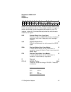
EMS Enable Memory Space 1
This bit controls the ability of the LSI53C875A to respond
to Memory space accesses. A value of zero disables the
device response. A value of one allows the LSI53C875A
to respond to Memory Space accesses at the address
range specified by Base Address Register One (MEM-
ORY) and Base Address Register Two (SCRIPTS RAM)
registers in the PCI configuration space.
EIS Enable I/O Space 0
This bit controls the LSI53C875A response to I/O space
accesses. A value of zero disables the device response.
A value of one allows the LSI53C875A to respond to I/O
Space accesses at the address range specified by the
Base Address Register Zero (I/O) register in the PCI
configuration space.


