2-34 Functional Description
situation may occur when a SCSI controller (operating in the initiator
mode) tries to select a target and is reselected by another. The Select
SCRIPTS instruction has an alternate address to which the SCRIPTS will
jump when this situation occurs. The analogous situation for target
devices is being selected while trying to perform a reselection.
Once a change in operating mode occurs, the initiator SCRIPTS should
start with a Set Initiator instruction or the target SCRIPTS should start
with a Set Target instruction. The Selection and Reselection Enable bits
(SCSI Chip ID (SCID) bits 5 and 6, respectively) should both be asserted
so that the LSI53C875A may respond as an initiator or as a target. If only
selection is enabled, the LSI53C875A cannot be reselected as an
initiator. There are also status and interrupt bits in the SCSI Interrupt
Status Zero (SIST0) and SCSI Interrupt Enable Zero (SIEN0) registers,
respectively, indicating that the LSI53C875A has been selected (bit 5)
and reselected (bit 4).
2.2.15 Synchronous Operation
The LSI53C875A can transfer synchronous SCSI data in both the
initiator and target modes. The SCSI Transfer (SXFER) register controls
both the synchronous offset and the transfer period. It may be loaded by
the CPU before SCRIPTS execution begins, from within SCRIPTS using
a Table Indirect I/O instruction, or with a Read-Modify-Write instruction.
The LSI53C875A can receive data from the SCSI bus at a synchronous
transfer period as short as 50 ns, regardless of the transfer period used
to send data. The LSI53C875A can receive data at one-fourth of the
divided SCLK frequency. Depending on the SCLK frequency, the
negotiated transfer period, and the synchronous clock divider, the
LSI53C875A can send synchronous data at intervals as short as 50 ns
for Ultra SCSI, 100 ns for fast SCSI and 200 ns for SCSI-1.
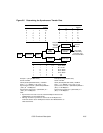
2.2.15.1 Determining the Data Transfer Rate
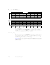
Synchronous data transfer rates are controlled by bits in two different
registers of the LSI53C875A. Following is a brief description of the bits.
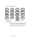
Figure 2.6 illustrates the clock division factors used in each register, and
the role of the register bits in determining the transfer rate.


