SCSI Registers 4-83
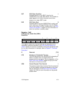
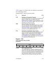
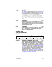
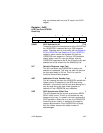
LEDC LED_CNTL 5
The internal connected signal (bit 3 of the Interrupt Status
Zero (ISTAT0) register) will be presented on GPIO0 if this
bit is set and bit 6 of GPCNTL0 is cleared and the chip
is not in progress of performing an EEPROM
autodownload regardless of the state of bit 0 (GPIO0).
This provides a hardware solution to driving a SCSI
activity LED in many implementations of LSI Logic SCSI
chips.
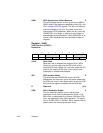
GPIO GPIO Enable [4:2]
General purpose control, corresponding to bits [4:2] in
the GPREG0 register and pins GPIO[4:2]. GPIO4 powers
up as a general purpose output, and GPIO[3:2] power-up
as general purpose inputs.
GPIO GPIO Enable [1:0]
These bits power-up set, causing the GPIO1 and GPIO0
pins to become inputs. Clearing these bits causes
GPIO[1:0] to become outputs.
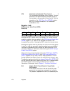
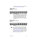
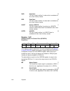
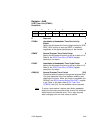
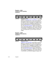
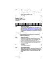
Register: 0x48
SCSI Timer Zero (STIME0)
Read/Write
HTH[3:0] Handshake-to-Handshake Timer Period [7:4]
These bits select the handshake-to-handshake time-out
period, the maximum time between SCSI handshakes
(SREQ/ to SREQ/ in target mode, or SACK/ to SACK/ in
initiator mode). When this timing is exceeded, an interrupt
is generated and the HTH bit in the SCSI Interrupt Status
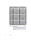
One (SIST1) register is set. The following table contains
time-out periods for the Handshake-to-Handshake Timer,
the Selection/Reselection Timer (bits [3:0]), and the
General Purpose Timer (SCSI Timer One (STIME1) bits
[3:0]). For a more detailed explanation of interrupts, refer
to Chapter 2, “Functional Description.”
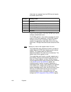
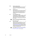
7430
HTH[3:0] SEL[3:0]
00000000


