LSI53C875A PCI to Ultra SCSI Controller 3-1
Chapter 3
Signal Descriptions
This chapter presents the LSI53C875A pin configuration and signal
definitions using tables and illustrations. This chapter contains the
following sections:
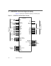
• Section 3.1, “LSI53C875A Functional Signal Grouping”
• Section 3.2, “Signal Descriptions”
• Section 3.3, “PCI Bus Interface Signals”
• Section 3.4, “SCSI Bus Interface Signals”
• Section 3.5, “GPIO Signals”
• Section 3.6, “ROM Flash and Memory Interface Signals”
• Section 3.7, “Test Interface Signals”
• Section 3.8, “Power and Ground Signals”
• Section 3.9, “MAD Bus Programming”
A slash (/) at the end of a signal name indicates that the active state
occurs when the signal is at a LOW voltage. When the slash is absent,
the signal is active at a HIGH voltage.


