


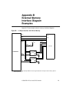
IX-4 Index
burst (Cont.)
length (BL[1:0]) 4-66
length bit 2 (BL2) 4-61
opcode fetch enable (BOF) 4-68
size selection 2-6
bus
command and byte enables 3-5
fault (BF) 4-40, 4-69
byte
count 5-37
empty in DMA FIFO (FMT) 4-53
full in DMA FIFO (FFL) 4-53
offset counter (BO) 4-57
C
cache line size 2-7, 2-9
(CLS) 4-7
enable (CLSE) 4-70
register 2-6
cache mode, see PCI cache mode 2-9
call instruction 5-27
Cap_ID (CID) 4-15
capabilities pointer (CP) 4-13
carry test 5-30
chained block moves 2-44
SCRIPTS instruction 2-47
SODL register 2-46
SWIDE register 2-46
wide SCSI receive bit 2-46
wide SCSI send bit 2-45
chained mode (CHM) 4-26
change bus phases 2-17
chip
control 0 (CCNTL0) 4-95
control 1 (CCNTL1) 4-97
revision level (V) 4-56
test five (CTEST5) 4-60
test one (CTEST1) 4-53
test six (CTEST6) 4-62
test three (CTEST3) 4-56
test two (CTEST2) 4-54
test zero (CTEST0) 4-53
type (TYP) 4-81
CHMOV 2-44
class code (CC) 4-7
clear DMA FIFO 2-42, 4-56
clear instruction 5-15, 5-17
clear SCSI FIFO (CSF) 4-92
CLF 2-42
CLK 3-4
clock 3-4
address incrementor (ADCK) 4-60
byte counter (BBCK) 4-61
conversion factor (CCF[2:0]) 4-29
quadrupler 2-20
CLSE 2-6, 2-7
CMP 2-39
compare
data 5-31
phase 5-31
configuration
read command 2-5
space 2-3
write command 2-5
configured
as I/O (CIO) 4-54
as memory (CM) 4-54
connected (CON) 4-24, 4-49
CSF 2-42
CTEST4 2-25
cumulative SCSI byte count (CSBC) 4-108
cycle frame 3-6
D
D1_Support (D1S) 4-16
D2_Support (D2S) 4-16
DACs 2-19
data
(DATA) 4-18
acknowledge status (DACK) 4-55
compare mask 5-31
compare value 5-32
parity error reported (DPR) 4-6
paths 2-28
request status (DREQ) 4-55
structure address (DSA) 4-47
transfer direction (DDIR) 4-54
data read (DRD) 4-82
data write (DWR) 4-82
data_scale (DSCL) 4-17
data_select (DSLT) 4-17
data-in 2-47
data-out 2-47
DCNTL 2-6, 2-39
decode of MAD pins 3-14
default download mode 2-50
destination
address 5-23
I/O memory enable (DIOM) 4-67
detected parity error (from slave) (DPE) 4-5
determining the data transfer rate 2-34
device
ID (DID) 4-3
select 3-6
specific initialization (DSI) 4-16
DEVSEL/ 3-6
timing (DT[1:0]) 4-5
DIEN 2-25, 2-39, 2-40
DIP 2-38, 2-41, 2-42, 2-43
direct 5-19
disable
auto FIFO clear (DISFC) 4-96
dual address cycle (DDAC) 4-97
halt on parity error or ATN (target only) (DHP) 4-23
internal load and store (DILS) 4-96
single initiator response (DSI) 4-92
disconnect 2-17
disconnect instruction 5-15
DMA
byte counter (DBC) 4-62
command (DCMD) 4-63
control (DCNTL) 4-70
direction (DDIR) 4-61
FIFO 2-8, 2-27, 2-38
(DF) 4-62
(DFIFO) 4-57
byte offset counter, bits [9:8] (BO[9:8]) 4-62
empty (DFE) 4-39
size (DFS) 4-61
interrupt 2-39, 2-40, 2-42
enable (DIEN) 4-69