4-100 Registers
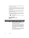
operation is performed, one of the six selector registers below will be
used to generate a 64-bit address.
If the selector for a particular device operation is zero, then a standard
32-bit address cycle will be generated. If the selector value is nonzero,
then a DAC will be issued and the 64-bit address will be presented in
two address phases.
All selectors default to 0 (zero) with the exception of the 16 SCRATCH
registers, these power-up in an indeterminate state and should be
initialized before they are used.
All selectors can be read/written using the Load and Store SCRIPTS
instruction, Memory-to-Memory Move, Read/Write SCRIPTS instruction,
or CPU with SCRIPTS not running.
Note:
Crossing of selector boundaries in one memory operation
is not supported.
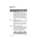
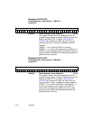
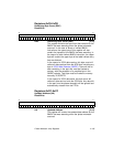
Registers:0xA0–0xA3
Memory Move Read Selector (MMRS)
Read/Write
MMRS Memory Move Read Selector (MMRS)
Supplies the upper Dword of a 64-bit address during data
read operations for Memory-to-Memory Moves and
absolute address LOAD operations.
A special mode of this register can be enabled by setting
the PCI Configuration Enable bit in the Ch ip Test Two
(CTEST2) register. Because the LSI53C875A supports
only a 32-bit memory mapped PCI base address, the
MMRS register is always read as 0x00000000 when in
the special mode.
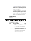
Writes to the MMRS register are unaffected. Clearing the
PCI Configuration Into Enable bit causes the MMRS
register to return to normal operation.
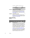
31 0
MMRS
00000000000000000000000000000000


