


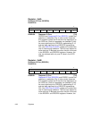
4-94 Registers
Register: 0x52
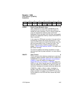
SCSI Test Four (STEST4)
Read Only
R Reserved [7:6]
LOCK Frequency Lock 5
This bit is used when enabling the SCSI clock quadrupler,
which allows the LSI53C875A to transfer data at Ultra
SCSI rates. Poll this bit for a 1 to determine that the clock
quadrupler has locked. For more information on enabling
the clock quadrupler, refer to the descriptions of SCSI
Test O ne (STES T1),bits2and3.
R Reserved [4:0]
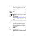
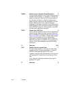
Register: 0x53
Reserved
Registers:0x54–0x55
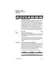
SCSI Output Data Latch (SODL)
Read/Write
SODL SCSI Output Data Latch [15:0]
This register is used primarily for diagnostic testing or
programmed I/O operation. Data written to this register is
asserted onto the SCSI data bus by setting the Assert
Data Bus bit in the SCSI Control One (SCNTL1) register.
This register is used to send data using programmed I/O.
Data flows through this register when sending data in any
mode. It is also used to write to the synchronous data
FIFO when testing the chip. The power-up value of this
register is indeterminate.
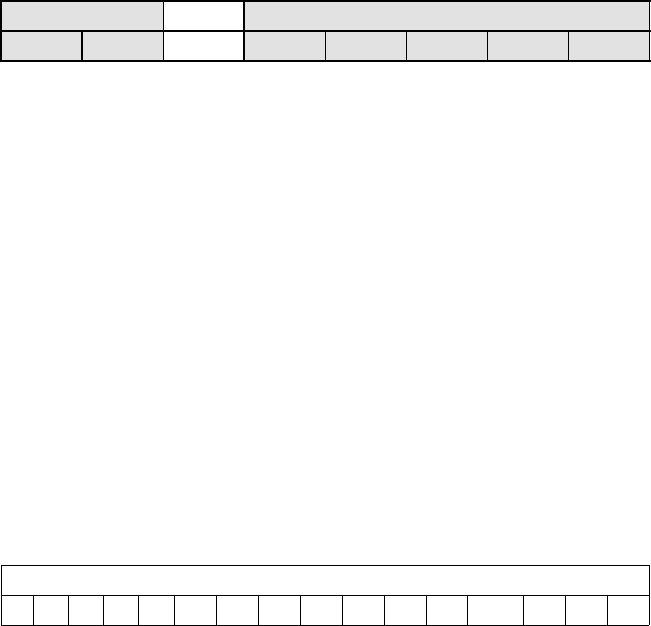
7654 0
RLOCK R
x x0x x x x x
15 0
SODL
xxxxx x x
x x xxx x xxx