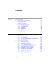
Contents xiii
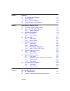
5.2 SCSI Information Transfer Phase 5-12
5.3 Read/Write Instructions 5-24
5.4 Transfer Control Instructions 5-26
5.5 SCSI Phase Comparisons 5-29
6.1 Absolute Maximum Stress Ratings 6-2
6.2 Operating Conditions 6-2
6.3 Input Capacitance 6-2
6.4 Bidirectional Signals—MAD[7:0], MAS/[1:0], MCE/, MOE/,
MWE/ 6-3
6.5 Bidirectional Signals—GPIO0_FETCH/, GPIO1_MASTER/,
GPIO[2:4] 6-3
6.6 Bidirectional Signals—AD[31:0], C_BE[3:0]/, FRAME/,
IRDY/, TRDY/, DEVSEL/, STOP/, PERR/, PAR 6-4
6.7 Input Signals—CLK, GNT/, IDSEL, RST/, SCLK, TCK,
TDI, TEST_HSC, TEST_RST, TMS, TRST/ 6-4
6.8 Output Signal—TDO 6-4
6.9 Output Signals—IRQ/, MAC/_TESTOUT, REQ/ 6-5
6.10 Output Signal—SERR/ 6-5
6.11 TolerANT Technology Electrical Characteristics for SE
SCSI Signals 6-6
6.12 External Clock 6-9
6.13 Reset Input 6-10
6.14 Interrupt Output 6-10
6.15 PCI Configuration Register Read 6-13
6.16 PCI Configuration Register Write 6-14
6.17 32-Bit Operating Register/SCRIPTS RAM Read 6-15
6.18 64-Bit Address Operating Register/SCRIPTS RAM Read 6-16
6.19 32-Bit Operating Register/SCRIPTS RAM Write 6-17
6.20 64-Bit Address Operating Register/SCRIPTS RAM Write 6-18
6.21 Nonburst Opcode Fetch, 32-Bit Address and Data 6-19
6.22 Burst Opcode Fetch, 32-Bit Address and Data 6-21
6.23 Back-to-Back Read, 32-Bit Address and Data 6-23
6.24 Back-to-Back Write, 32-Bit Address and Data 6-25
6.25 Burst Read, 32-Bit Address and Data 6-27
6.26 Burst Read, 64-Bit Address and Data 6-29
6.27 Burst Write, 32-Bit Address and Data 6-31
6.28 Burst Write, 64-Bit Address and 32-Bit Data 6-33
6.29 External Memory Read 6-35


