


ROM Flash and Memory Interface Signals 3-11
3.6 ROM Flash and Memory Interface Signals
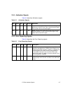
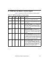
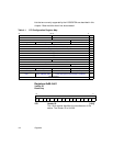
Table 3.1 2 describes the ROM Flash and Memory Interface signals.
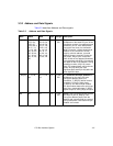
Table 3.12 ROM Flash and Memory Interface Signals
Name PQFP BGA Type Strength Description
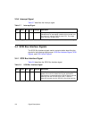
MWE/ 139 C7 O 4 mA Memory Write Enable. Thispinisusedasawrite
enable signal to an external flash memory.
MCE/ 141 A7 O 4 mA Memory Chip Enable. Thispinisusedasachip
enable signal to an external EEPROM or flash
memory device.
MOE/ 140 B7 O 4 mA Memory Output Enable. Thispinisusedasan
output enable signal to an external EEPROM or
flash memory during read operations. It is also
used to test the connectivity of the LSI53C875A
signals in test mode.
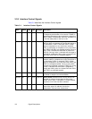
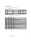
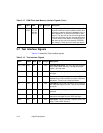
MAC/_
TESTOUT
77 L10 O 16 mA Memory Access Control. This pin can be
programmed to indicate local or system memory
accessed (non-PCI applications). It is also used to
test the connectivity of the LSI53C875A signals in
test mode.
MAS0/ 137 A8 O 4 mA Memory Address Strobe 0. This pin is used to
latch in the least significant address byte (bits [7:0])
of an external EEPROM or flash memory. Since
the LSI53C875A moves addresses eight bits at a
time, this pin connects to the clock of an external
bank of flip-flops which are used to assemble up to
a 20-bit address for the external memory.
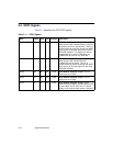
MAS1/ 136 B8 O 4 mA Memory Address Strobe 1. This pin is used to
latch in the most significant address byte (bits
[15:8]) of an external EEPROM or flash memory.
Since the LSI53C875A moves addresses eight bits
at a time, this pin connects to the clock of an
external bank of flip-flops which assemble up to a
20-bit address for the external memory.