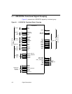
3-10 Signal Descriptions
3.5 GPIO Signals
Table 3.1 1 describes the SCSI GPIO signals.
Table 3.11 GPIO Signals
Name PQFP BGA Type Strength Description
GPIO0_FETCH/ 53 N5 I/O 8 mA SCSI General Purpose I/O pin. Optionally,
when driven LOW, indicates that the next bus
request will be for an opcode fetch. This pin is
programmable at power-up through the MAD7
pin to serve as the data signal for the serial
EEPROM interface. This signal can also be
programmedtobedrivenLOWwhenthe
LSI53C875A is active on the SCSI bus.
GPIO1_MASTER/ 54 K6 I/O 8 mA SCSI General Purpose I/O pin. Optionally,
when driven LOW, indicates that the
LSI53C875A is bus master. This pin is
programmable at power-up through the MAD7
pin to serve as the clock signal for the serial
EEPROM interface.
GPIO2 68 J8 I/O 8 mA SCSI General Purpose I/O pin. This pin
powers up as an input.
GPIO3 70 M9 I/O 8 mA SCSI General Purpose I/O pin. This pin
powers up as an input.
GPIO4 71 L9 I/O 8 mA SCSI General Purpose I/O pin. GPIO4
powers up as an output. (This pin may be used
as the enable line for VPP, the 12 V power
supply to the external flash memory interface.)


