4-104 Registers
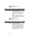
Registers:0xC0–0xC3
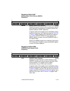
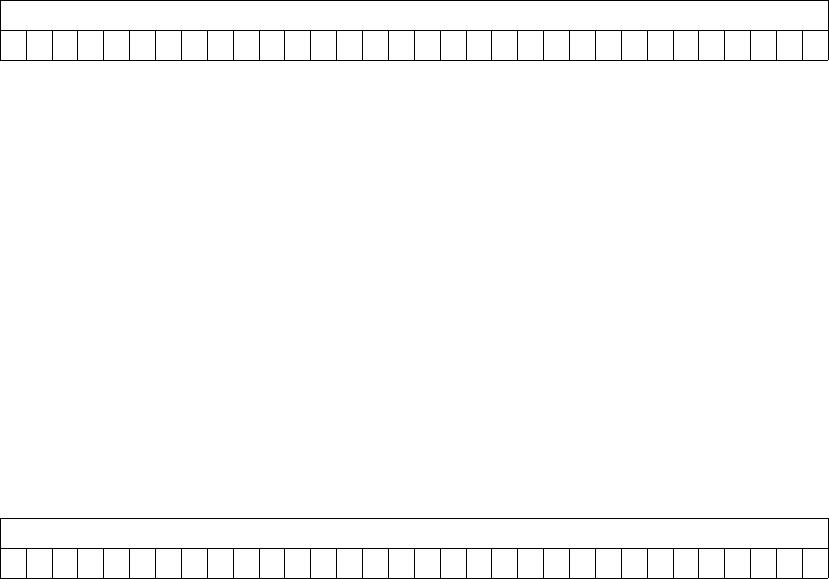
PhaseMismatchJumpAddress1(PMJAD1)
Read/Write
PMJAD1 Phase Mismatch Jump Address 1 [31:0]
This register contains the 32-bit address that will be
jumped to upon a phase mismatch. Depending upon the
state of the PMJCTL bit in register Chip Control 0
(CCNTL0) this address will either be used during an
outbound (data out, command, message out) phase
mismatch
(PMJCTL = 0) or when the WSR bit is cleared
(PMJCTL = 1). It should be loaded with an address of a
SCRIPTS routine that will handle the updating of memory
data structures of the BMOV that was executing when the
phase mismatch occurred.
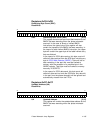
Registers:0xC4–0xC7
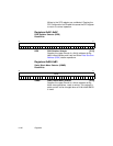
PhaseMismatchJumpAddress2(PMJAD2)
Read/Write
PMJAD2 Phase Mismatch Jump Address 2 [31:0]
This register contains the 32-bit address that will be
jumped to upon a phase mismatch. Depending upon the
state of the PMJCTL bit in register Chip Control 0
(CCNTL0) this address will either be used during an
inbound (data in, status, message in) phase mismatch
(PMJCTL = 0) or when the WSR bit is set (PMJCTL = 1).
It should be loaded with an address of a SCRIPTS
routine that will handle the updating of memory data
structures of the BMOV that was executing when the
phase mismatch occurred.
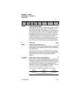
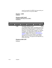
31 0
PMJAD1
00000000000000000000000000000000
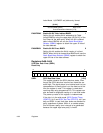
31 0
PMJAD2
00000000000000000000000000000000


