


4-60 Registers
LSI53C875A is informed of the error by the PERR/ pin
being asserted by the target. When this bit is cleared, the
LSI53C875A does not interrupt if a master parity error
occurs. This bit is cleared at power-up.
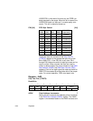
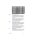
FBL[2:0] FIFO Byte Control [2:0]
These bits steer the contents of the Chip Test Six
(CTEST6) register to the appropriate byte lane of the
64-bit DMA FIFO. If the FBL3 bit is set, then FBL2
through FBL0 determine which of eight byte lanes can be
read or written. When cleared, the byte lane read or
written is determined by the current contents of the DMA
Next Address (DNAD) and DMA Byte Counter (DBC)
registers. Each of the eight bytes that make up the 64-bit
DMA FIFO is accessed by writing these bits to the proper
value. For normal operation, FBL3 must equal zero.
Register: 0x22
Chip Test Five (CTEST5)
Read/Write
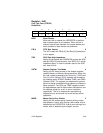
ADCK Clock Address Incrementor 7
Setting this bit increments the address pointer contained
in the DMA Next Address (DNAD) register. The DNAD
register is incremented based on the DNAD contents and
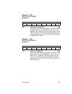
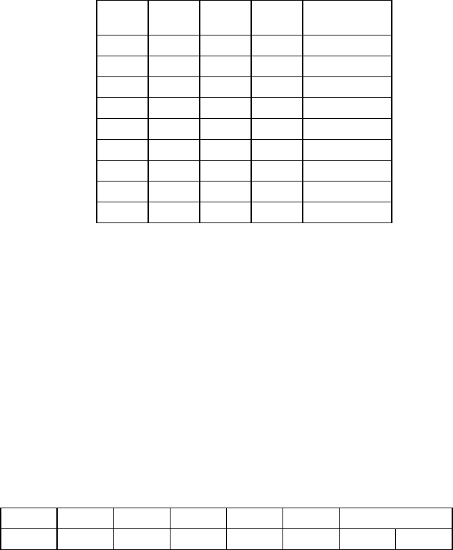
FBL3 FBL2 FBL1 FBL0
DMA FIFO
Byte Lane
0 x x x Disabled
1000 0
1001 1
1010 2
1011 3
1100 4
1101 5
1110 6
1111 7
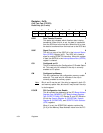
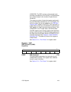
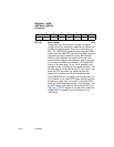
76543210
ADCK BBCK DFS MASR DDIR BL2 BO[9:8]
00000000