


SCSI Registers 4-67
SIOM Source I/O Memory Enable 5
This bit is defined as an I/O Memory Enable bit for the
source address of a Memory Move or Block Move
Command. If this bit is set, then the source address is in
I/O space; and if cleared, then the source address is in
memory space.
This function is useful for register-to-memory operations
using the Memory Move instruction when the
LSI53C875A is I/O mapped. Bits 4 and 5 of the Chip Test
Two (CTE ST2) register are used to determine the
configuration status of the LSI53C875A.
DIOM Destination I/O Memory Enable 4
This bit is defined as an I/O Memory Enable bit for the
destination address of a Memory Move or Block Move
Command. If this bit is set, then the destination address
is in I/O space; and if cleared, then the destination
address is in memory space.
This function is useful for memory-to-register operations
using the Memory Move instruction when the
LSI53C875A is I/O mapped. Bits 4 and 5 of the Chip Test
Two (CTE ST2) register are used to determine the
configuration status of the LSI53C875A.
ERL Enable Read Line 3
This bit enables a PCI Read Line command. If this bit is
set and the chip is about to execute a read cycle other
than an opcode fetch, then the command is 0b1110.
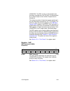
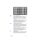
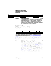
BL2
(CTEST5 bit 2) BL1 BL0
Burst Length
Transfers Dwords
0002 4
0014 8
010816
0111632
1
1003264
1
10164128
1
11064128
1
1 1 1 Reserved Reserved
1. The 944-byte FIFO must be enabled for these burst sizes.