


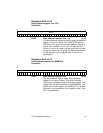
PCI Configuration Registers 4-9
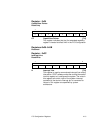
Registers:0x10–0x13
Base Address Register Zero (I/O)
Read/Write
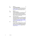
BAR0 Base Address Register Zero - I/O [31:0]
This base address register is used to map the operating
register set into I/O space. The LSI53C875A requires
256 bytes of I/O space for this base address register. It
has bit zero hardwired to one. Bit 1 is reserved and
returns a zero on all reads, and the other bits are used
to map the device into I/O space. For detailed information
on the operation of this register, refer to the PCI 2.2
specification.
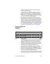
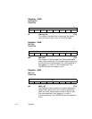
Registers:0x14–0x17
Base Address Register One (MEMORY)
Read/Write
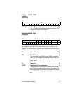
BAR1 Base Address Register One [31:0]
This base address register maps SCSI operating
registers into memory space. This device requires
1024 bytes of address space for this base register. This
register has bits [9:0] hardwired to 0b0000000000. The
default value of this register is 0x00000000. For detailed
information on the operation of this register, refer to the
PCI 2.2 specification.
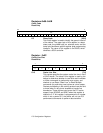
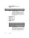
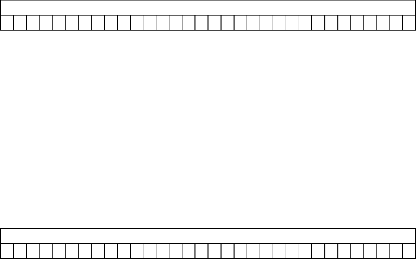
31 0
BAR0
00000000000000000000000000000001
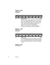
31 0
BAR1
00000000000000000000000000000000