


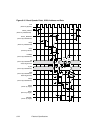
PCI and External Memory Interface Timing Diagrams 6-17
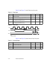
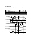
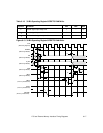
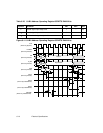
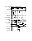
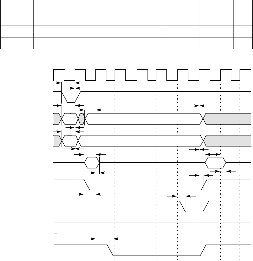
Figure 6.13 32-Bit Operating Register/SCRIPTS RAM Write
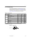
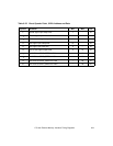
Table 6.19 32-Bit Operating Register/SCRIPTS RAM Write
Symbol Parameter Min Max Unit
t
1
Shared signal input setup time 7 – ns
t
2
Shared signal input hold time 0 – ns
t
3
CLK to shared signal output valid – 11 ns
CLK
(Driven by System)
FRAME/
(Driven by Master)
AD
(Driven by Master)
C_BE/
(Driven by Master)
PA R
(Driven by Master)
IRDY/
(Driven by Master)
TRDY/
(Driven by LSI53C875A)
STOP/
(Driven by LSI53C875A)
DEVSEL/
(Driven by LSI53C875A)
Addr
In
CMD
In
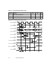
t
3
In
t
1
t
1
t
1
t
1
t
1
t
1
t
2
t
2
t
2
t
2
t
2
t
2
t
1
t
3
t
2
t
2