


4-10 Registers
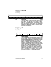
Registers:0x18–0x1B
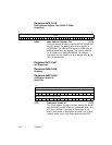
Base Address Register Two (SCRIPTS RAM)
Read/Write
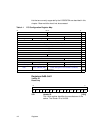
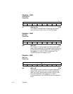
BAR2 Base Address Register Two [31:0]
This base register is used to map the SCRIPTS RAM into
memory space. The default value of this register is
0x00000000. The LSI53C875A points to 4096 bytes of
address space with this register. This register has bits
[11:0] hardwired to 0b000000000000. For detailed
information on the operation of this register, refer to the
PCI 2.2 specification.
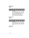
Registers:0x1C–0x27
Not Supported
Registers:0x28–0x2B
Reserved
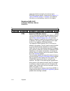
Registers:0x2C–0x2D
Subsystem Vendor ID
Read Only
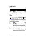
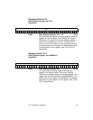
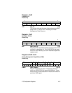
SVID Subsystem Vendor ID [15:0]
This 16-bit register is used to uniquely identify the vendor
manufacturing the add-in board or subsystem where this
PCI device resides. It provides a mechanism for an
add-in card vendor to distinguish its cards from another
vendor’s cards, even if the cards have the same PCI
31 0
BAR2
00000000000000000000000000000000
15 0
SVID
If MAD[7] HIGH Default
0001000000000000
If MAD[7] LOW See Description Default
xxxxxxxxxxxxxxxx