


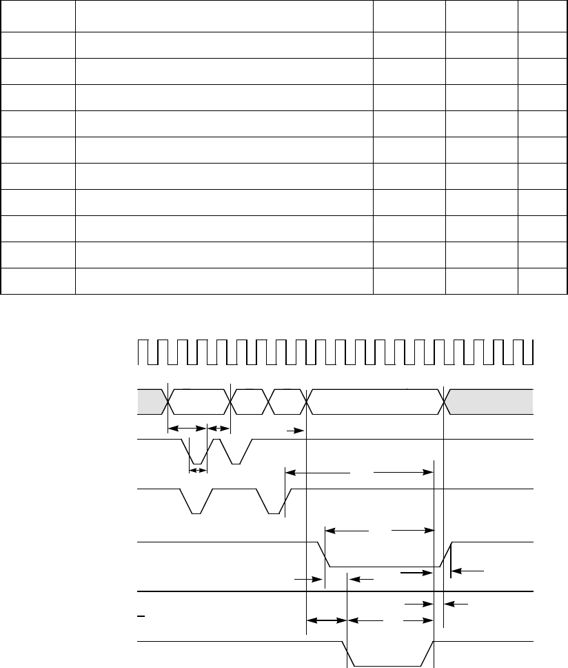
PCI and External Memory Interface Timing Diagrams 6-43
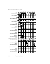
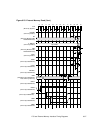
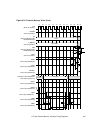
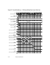
Figure 6.26 Normal/Fast Memory (≥=128 Kbytes) Single Byte Access Write Cycle
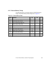
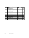
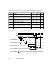
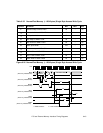
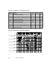
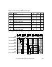
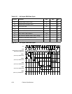
Table 6.32 Normal/Fast Memory (
≥=128 Kbytes) Single Byte Access Write Cycle
Symbol Parameter Min Max Unit
t
11
Address setup to MAS/ HIGH 25 – ns
t
12
Address hold from MAS/ HIGH 15 – ns
t
13
MAS/ pulse width 25 – ns
t
20
Data setup to MWE/ LOW 30 – ns
t
21
Data hold from MWE/ HIGH 20 – ns
t
22
MWE/ pulse width 100 – ns
t
23
Address setup to MWE/ LOW 60 – ns
t
24
MCE/ LOW to MWE/ HIGH 120 – ns
t
25
MCE/ LOW to MWE/ LOW 25 – ns
t
26
MWE/ HIGH to MCE/ HIGH 25 – ns
CLK
MAD
(Driven by LSI53C875A)
MAS1/
(Driven by LSI53C875A)
MAS0/
(Driven by LSI53C875A)
MCE/
(Driven by LSI53C875A)
MOE/
(Driven by LSI53C875A)
MWE/
(Driven by LSI53C875A)
t
11
t
12
t
13
t
23
t
24
t
20
Higher
Address
1. 2.
1. Middle Address 2. Lower Address
Valid Write Data
t
22
t
21
t
26
t
25