4-88 Registers
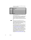
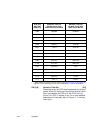
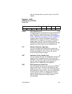
SOM SCSI Synchronous Offset Maximum 0
This bit indicates that the current synchronous SREQ/,
SACK/ offset is the maximum specified by bits [3:0] in the
SCSI Transfer (SXFER) register. This bit is not latched
and may change at any time. It is used in low level
synchronous SCSI operations. When this bit is set, the
LSI53C875A, as a target, is waiting for the initiator to
acknowledge the data transfers. If the LSI53C875A is an
initiator, then the target has sent the offset number of
requests.
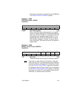
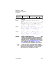
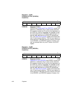
Register: 0x4D
SCSI Test One (STEST1)
Read/Write
SCLK SCSI Clock 7
When set, this bit disables the external SCLK (SCSI
Clock) pin, and the chip uses the PCI clock as the
internal SCSI clock. When set, it will also select the PCI
clock as the internal SCSI clock if the internal clock
quadrupler is enabled and selected.
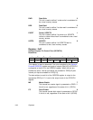
ISO SCSI Isolation Mode 6
This bit allows the LSI53C875A to put the SCSI
bidirectional and input pins into a low power mode when
the SCSI bus is not in use. When this bit is set, the SCSI
bus inputs are logically isolated from the SCSI bus.
R Reserved [5:4]
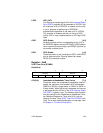
QEN SCLK Quadrupler Enable 3
This bit, when set, powers up the internal clock
quadrupler circuit, which quadruples the SCLK. A 40
MHz clock is quadrupled to an internal 160 MHz SCSI
clock, as required for Ultra SCSI operation. The output
from a 20 MHz SCLK is 80 MHz. When cleared, this bit
powers down the internal quadrupler circuit.
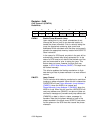
76543210
SCLK ISO
RQENQSELR
00
x x00x x


