4-36 Registers
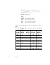
is also possible to program these signals as live inputs
and sense them through a SCRIPTS register to register
Move Instruction. GPIO4 may be used to enable or
disable V
PP
, the 12 Volt power supply to the external flash
memory. This bit powers up with the power to external
memory disabled. GPIO[3:0] default as inputs and GPIO4
defaults as an output pin. When configured as inputs, an
internal pull-down is enabled for GPIO[4:2]. For
GPIO[1:0], internal pull-ups are enabled.
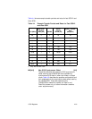
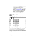
LSI Logic software uses the GPIO[1:0] signals to access
serial EEPROM. GPIO1 is used as a clock, with the
GPIO0 pin serving as data.
LSI Logic software also reserves the use of GPIO[4:2]. If
there is a need to use GPIO[4:2] please check with LSI
Logic for additional information.
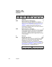
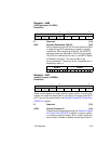
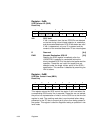
Register: 0x08
SCSI First Byte Received (SFBR)
Read/Write
SFBR SCSI First Byte Received [7:0]
This register contains the first byte received in any
asynchronous information transfer phase. For example,
when a LSI53C875A is operating in the initiator mode,
this register contains the first byte received in the
Message-In, Status phase, and Data-In phases.
When a Block Move instruction is executed for a
particular phase, the first byte received is stored in this
register, even if the present phase is the same as the last
phase. The first byte received for a particular input phase
is not valid until after a MOVE instruction is executed.
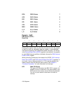
This register is also the accumulator for register read-
modify-writes with the SFBR as the destination. This
allows bit testing after an operation.
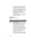
The SFBR is not writable using the CPU, and therefore
not by a Memory Move. However, it can be loaded using
SCRIPTS Read/Write operations. To load the SFBR with
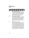
7 0
SFBR
00000000


