


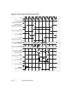

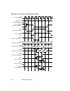
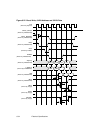

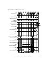
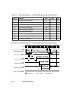
PCI and External Memory Interface Timing Diagrams 6-35
6.4.3 External Memory Timing
The tables and figures in this section describe LSI53C875A external
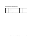
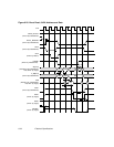
timings. The External Memory Write timings start on page 6-40.
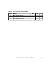
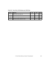
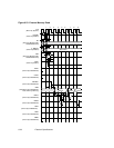
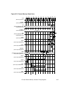
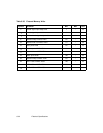
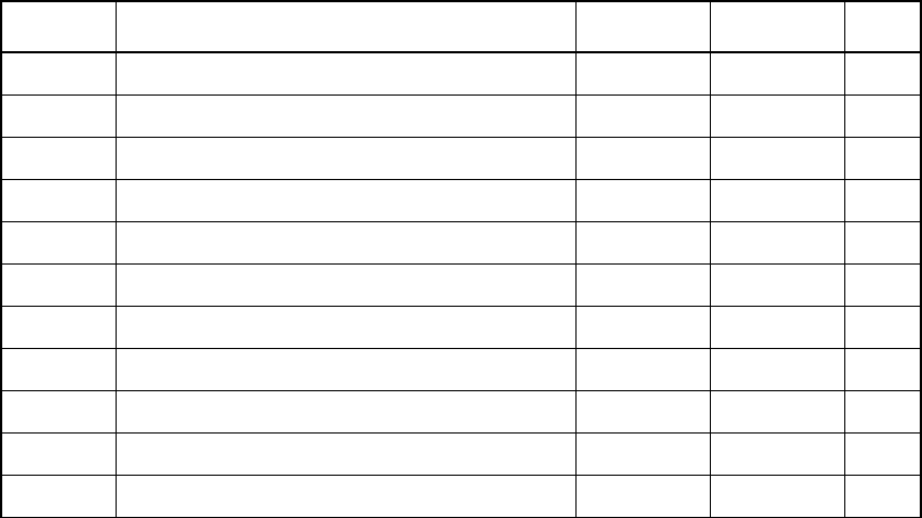
Table 6.29 External Memory Read
Symbol Parameter Min Max Unit
t
1
Shared signal input setup time 7 – ns
t
2
Shared signal input hold time 0 – ns
t
3
CLK to shared signal output valid – 11 ns
t
11
Address setup to MAS/ HIGH 25 – ns
t
12
Address hold from MAS/ HIGH 15 – ns
t
13
MAS/ pulse width 25 – ns
t
14
MCE/LOWtodataclockedin 150 – ns
t
15
Address valid to data clocked in 205 – ns
t
16
MOE/LOWtodataclockedin 100 – ns
t
17
Data hold from address, MOE/, MCE/ change 0 – ns
t
19
Data setup to CLK HIGH 5 – ns