


Power and Ground Signals 3-13
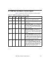
3.8 Power and Ground Signals
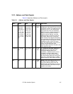
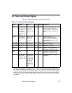
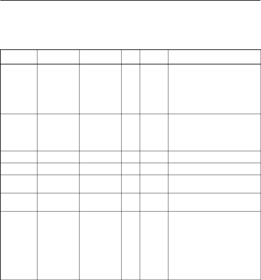
Table 3.1 4 describes the Power and Ground signals.
Table 3.14 Power and Ground Signals
Name PQFP BGA Type Strength Description
VSS_I/O 4, 10, 14, 18,
23, 27, 31, 37,
42, 48, 69, 79,
88, 93, 99,
104, 109, 114,
123, 133, 152,
158
A9,B11,D12,
E13, F12,
G11, J13,
K10, K12, N9
G N/A Ground for PCI bus
drivers/receivers, SCSI bus
drivers/receivers, local memory
interface drivers, and other I/O
pins.
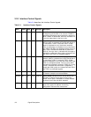
VDD_I/O 8, 21, 33, 45,
63, 74, 84,
118, 128, 138,
155
B10, C12, D2,
D5, E8, G1,
J5, J7, K1,
L11, M10
P N/A Power for PCI bus
drivers/receivers, SCSI bus
drivers/receivers, local memory
interface drivers/receivers, and
other I/O pins.
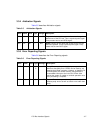
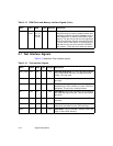
VDD_CORE 51, 83, 149 A5, L5, L12 P N/A Power for core logic.
VSS_CORE 55, 80, 146 C6, L6, N12 G N/A Ground for core logic.
VDDA 129 D9 P N/A Power for analog cells (clock
quadrupler and diffsense logic).
VSSA 132 B9 G N/A Ground for analog cells (clock
quadrupler and diffsense logic).
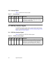
NC 72, 73, 75, 76,
78, 81, 82,
119–122, 124,
125, 134, 135
A12, A13, B2,
B3, B12, B13,
C3, C8, C11,
D1, D8, D10,
E9, F4-6, G5,
H4, H8, J3,
K3, K9, M2,
M4, M11-13,
N2, N10, N11,
N13
N/A N/A These pins have NO internal
connection.
Note:
The I/O driver pad rows and digital core have isolated power supplies as indicated by the “I/O”
and “CORE” extensions on their respective V
SS
and V
DD
names. These power and ground pins
should be connected directly to the primary power and ground planes of the circuit board. Bypass
capacitors of 0.01 µF should be applied between adjacent V
SS
and V
DD
pairs wherever possible.
Do not connect bypass capacitors between V
SS
and V
DD
pairs that cross power and ground bus
boundaries.