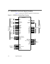
2-52 Functional Description
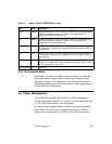
The LSI53C875A power states shown in Tabl e 2.8 are independently
controlled through two power state bits that are located in the PCI Power
Management Control/Status (PMCSR) register 0x44.
Although the PCI Bus Power Management Interface Specification does
not allow power state transitions D2 to D1, D3 to D2, or D3 to D1, the
LSI53C875A hardware places no restriction on transitions between
power states.
As the device transitions from one power level to a lower one, the
attributes that occur from the higher power state level are carried over
into the lower power state level. For example, D1 disables the SCSI CLK.
Therefore, D2 will include this attribute as well as the attributes defined
in the Power State D2 section. The PCI Function Power States D0, D1,
D2, and D3 are described below. Power state actions are separate for
each function.
2.5.1 Power State D0
Power state D0 is the maximum power state and is the power-up default
state. The LSI53C875A is fully functional in this state.
2.5.2 Power State D1
Power state D1 is a lower power state than D0. In this state, the
LSI53C875A core is placed in the snooze mode and the SCSI CLK is
disabled. In the snooze mode, a SCSI reset does not generate an IRQ/
signal. However, the SCSI CLK is still disabled.
Table 2.8 Power States
Configuration Register 0x44
Bits [1:0] Power State Function
00 D0 Maximum Power
01 D1 Disables SCSI Clock
10 D2 Coma Mode
11 D3 Minimum Power


