4-54 Registers
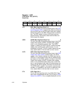
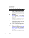
Register: 0x1A
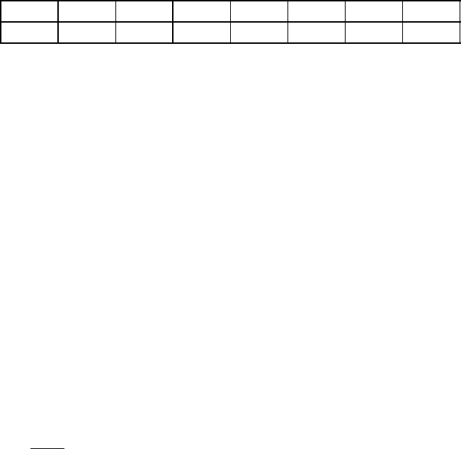
Chip Test Two (CTEST2)
Read Only (bit 3 write)
DDIR Data Transfer Direction 7
This status bit indicates which direction data is being
transferred. When this bit is set, the data is transferred
from the SCSI bus to the host bus. When this bit is clear,
the data is transferred from the host bus to the SCSI bus.
SIGP Signal Process 6
This bit is a copy of the SIGP bit in the Interrupt Status
Zero (ISTAT0) register (bit
=5). The SIGP bit is used to
signal a running SCRIPTS instruction. When this register
is read, the SIGP bit in the Interrupt Status Zero (ISTAT0)
register is cleared.
CIO Configured as I/O 5
This bit is defined as the Configuration I/O Enable Status
bit. This read only bit indicates if the chip is currently
enabled as I/O space.
CM Configured as Memory 4
This bit is defined as the configuration memory enable
status bit. This read only bit indicates if the chip is
currently enabled as memory space.
Note:
Bits 4 and 5 may be set if the chip is mapped in both I/O
and memory space. Also, bits 4 and 5 may be set if the chip
is dual-mapped.
PCICIE PCI Configuration Into Enable 3
This bit controls the shadowing of the PCI Base Address
Register One (MEMORY),PCIBase Address Register
Two (SCRIPTS RAM),PCIDeviceID,andPCIRevision
ID into the Scratch Register A (SCRATCHA), Scratch
Register B (SCRATCHB), and SCRIPTS Fetch Selector
(SFS) registers.
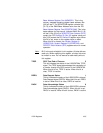
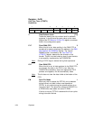
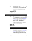
When it is set, the SCRATCHA register contains bits
[31:0] of the Memory Base Address value from the PCI
76543210
DDIR SIGP CIO CM PCICIE TEOP DREQ DACK
00xx0001


