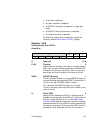
SCSI Registers 4-59
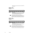
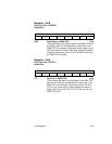
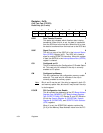
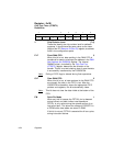
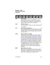
Register: 0x21
Chip Test Four (CTEST4)
Read/Write
BDIS Burst Disable 7
When set, this bit causes the LSI53C875A to perform
back-to-back cycles for all transfers. When this bit is
cleared, back-to-back transfers for opcode fetches and
burst transfers for data moves are performed.
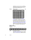
FBL3 FIFO Byte Control 6
This bit is used with FBL[2:0]. See Bits [2:0] description
in this register.
ZSD SCSI Data High Impedance 5
Setting this bit causes the LSI53C875A to place the SCSI
data bus SD[15:0] and the parity lines SDP[1:0] in a high
impedance state. In order to transfer data on the SCSI
bus, clear this bit.
SRTM Shadow Register Test Mode 4
Setting this bit allows access to the shadow registers
used by Memory-to-Memory Move operations. When this
bit is set, register accesses to the Temporary (TEMP) and
Data Structure Address (DSA) registers are directed to
the shadow copies STEMP (Shadow TEMP) and SDSA
(Shadow DSA). The registers are shadowed to prevent
them from being overwritten during a Memory-to-Memory
Move operation. The DSA and TEMP registers contain
the base address used for table indirect calculations, and
the address pointer for a call or return instruction,
respectively. This bit is intended for manufacturing
diagnostics only and should not be set during normal
operations.
MPEE Master Parity Error Enable 3
Setting this bit enables parity checking during master
data phases. A parity error during a bus master read is
detected by the LSI53C875A. A parity error during a bus
master write is detected by the target, and the
765432 0
BDIS FBL3 ZSD SRTM MPEE FBL[2:0]
00000000


