


Flash Memory Introduction
5-2
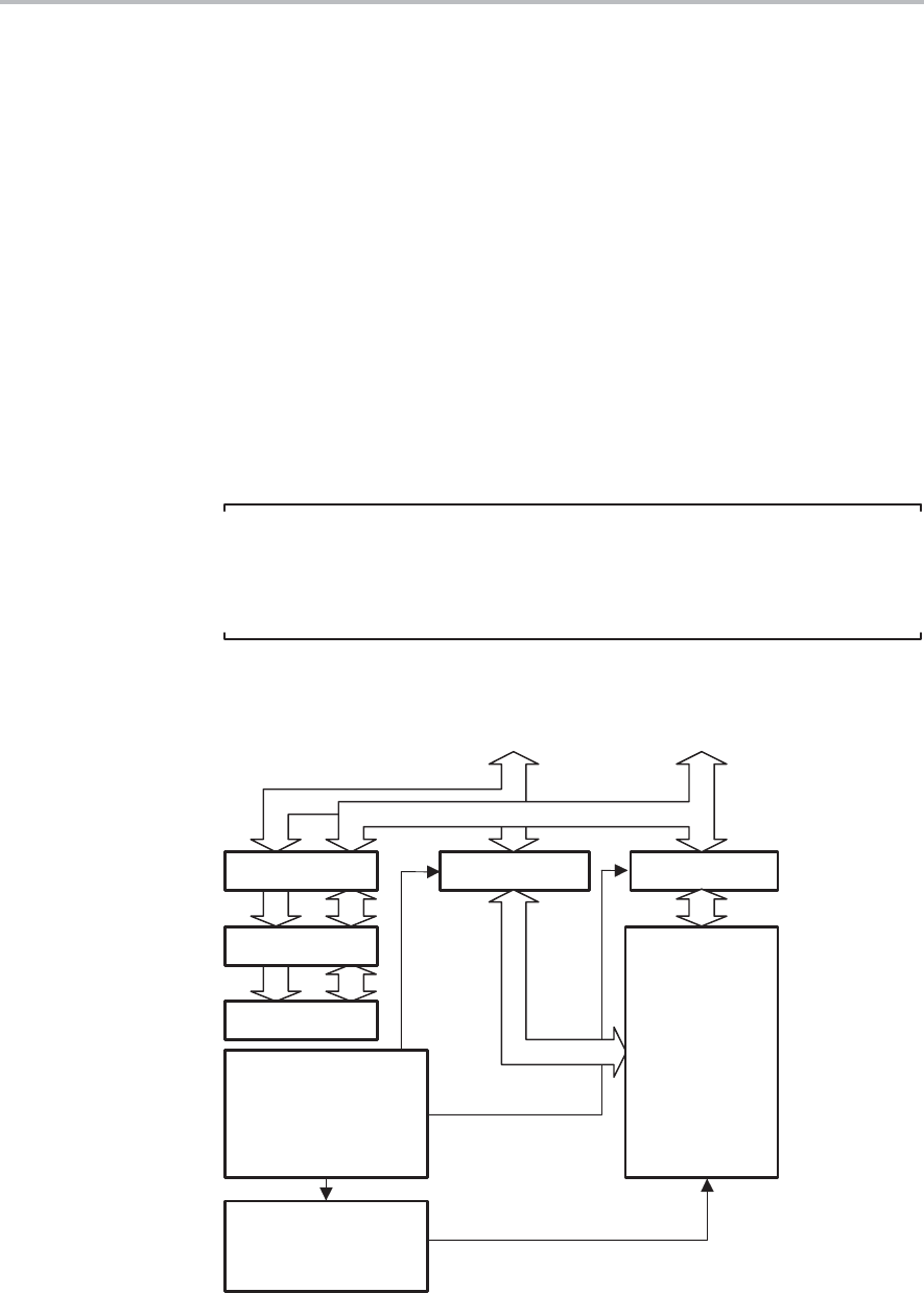
Flash Memory Controller
5.1 Flash Memory Introduction
The MSP430 flash memory is bit-, byte-, and word-addressable and
programmable. The flash memory module has an integrated controller that
controls programming and erase operations. The controller has three
registers, a timing generator, and a voltage generator to supply program and
erase voltages.
MSP430 flash memory features include:
- Internal programming voltage generation
- Bit, byte or word programmable
- Ultralow-power operation
- Segment erase and mass erase
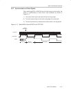
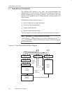
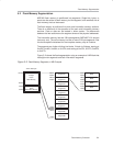
The block diagram of the flash memory and controller is shown in Figure 5−1.
Note: Minimum V
CC
During Flash Write or Erase
The minimum V
CC
voltage during a flash write or erase operation is 2.7 V.
If V
CC
falls below 2.7 V during a write or erase, the result of the write or erase
will be unpredictable.
Figure 5−1. Flash Memory Module Block Diagram
Enable
Data Latch
Enable
Address
Latch
Address Latch
Data Latch
MAB
MDB
FCTL1
FCTL2
FCTL3
Timing
Generator
Programming
Voltage
Generator
Flash
Memory
Array