


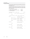
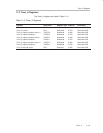

Timer_A Registers
11-22
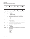
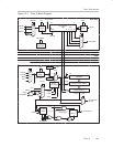
Timer_A
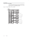
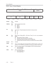
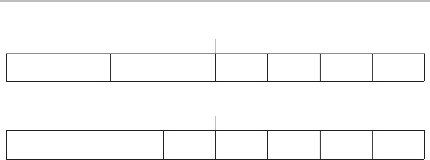
TACCTLx, Capture/Compare Control Register
15 14 13 12 11 10 9 8
CMx CCISx SCS SCCI Unused CAP
rw−(0) rw−(0) rw−(0) rw−(0) rw−(0) r−(0) r−(0) rw−(0)
76543210
OUTMODx CCIE CCI OUT COV CCIFG
rw−(0) rw−(0) rw−(0) rw−(0) r rw−(0) rw−(0) rw−(0)
CMx
Bit
15-14
Capture mode
00 No capture
01 Capture on rising edge
10 Capture on falling edge
11 Capture on both rising and falling edges
CCISx
Bit
13-12
Capture/compare input select. These bits select the TACCRx input signal.
See the device-specific datasheet for specific signal connections.
00 CCIxA
01 CCIxB
10 GND
11 V
CC
SCS
Bit 11 Synchronize capture source. This bit is used to synchronize the capture input
signal with the timer clock.
0 Asynchronous capture
1 Synchronous capture
SCCI
Bit 10 Synchronized capture/compare input. The selected CCI input signal is
latched with the EQUx signal and can be read via this bit
Unused
Bit 9 Unused. Read only. Always read as 0.
CAP
Bit 8 Capture mode
0 Compare mode
1 Capture mode
OUTMODx
Bits
7-5
Output mode. Modes 2, 3, 6, and 7 are not useful for TACCR0 because EQUx
= EQU0.
000 OUT bit value
001 Set
010 Toggle/reset
011 Set/reset
100 Toggle
101 Reset
110 Toggle/set
111 Reset/set