


DAC12 Operation
19-5
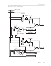
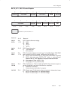
DAC12
19.2.2 DAC12 Reference
The reference for the DAC12 is configured to use either an external reference
voltage or the internal 1.5-V/2.5-V reference from the ADC12 module with the
DAC12SREFx bits. When DAC12SREFx = {0,1} the V
REF+
signal is used as
the reference and when DAC12SREFx = {2,3} the Ve
REF+
signal is used as the
reference.
To use the ADC12 internal reference, it must be enabled and configured via
the applicable ADC12 control bits (see the ADC12 chapter). Once the ADC12
reference is configured, the reference voltage appears on the V
REF+
signal.
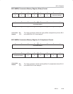
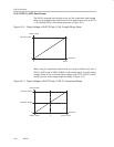
DAC12 Reference Input and Voltage Output Buffers
The reference input and voltage output buffers of the DAC12 can be
configured for optimized settling time vs power consumption. Eight
combinations are selected using the DAC12AMPx bits. In the low/low setting,
the settling time is the slowest, and the current consumption of both buffers is
the lowest. The medium and high settings have faster settling times, but the
current consumption increases.
See the device-specific data sheet for
parameters.
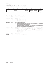
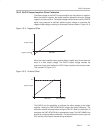
19.2.3 Updating the DAC12 Voltage Output
The DAC12_xDAT register can be connected directly to the DAC12 core or
double buffered. The trigger for updating the DAC12 voltage output is selected
with the DAC12LSELx bits.
When DAC12LSELx = 0 the data latch is transparent and the DAC12_xDAT
register is applied directly to the DAC12 core. the DAC12 output updates
immediately when new DAC12 data is written to the DAC12_xDAT register,
regardless of the state of the DAC12ENC bit.
When DAC12LSELx = 1, DAC12 data is latched and applied to the DAC12
core after new data is written to DAC12_xDAT. When DAC12LSELx = 2 or 3,
data is latched on the rising edge from the Timer_A CCR1 output or Timer_B
CCR2 output respectively. DAC12ENC must be set to latch the new data when
DAC12LSELx > 0.