


Timer_B Registers
12-23
Timer_B
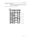
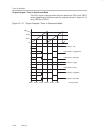
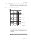
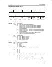
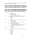
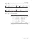
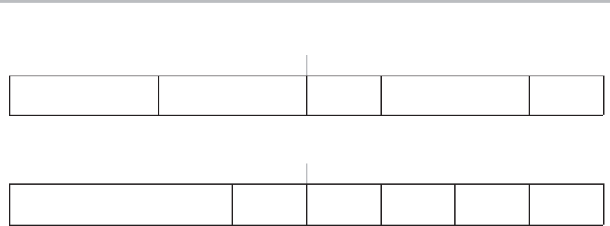
TBCCTLx, Capture/Compare Control Register
15 14 13 12 11 10 9 8
CMx CCISx SCS CLLDx CAP
rw−(0) rw−(0) rw−(0) rw−(0) rw−(0) rw−(0) r−(0) rw−(0)
76543210
OUTMODx CCIE CCI OUT COV CCIFG
rw−(0) rw−(0) rw−(0) rw−(0) r rw−(0) rw−(0) rw−(0)
CMx
Bit
15-14
Capture mode
00 No capture
01 Capture on rising edge
10 Capture on falling edge
11 Capture on both rising and falling edges
CCISx
Bit
13-12
Capture/compare input select. These bits select the TBCCRx input signal.
See the device-specific datasheet for specific signal connections.
00 CCIxA
01 CCIxB
10 GND
11 V
CC
SCS
Bit 11 Synchronize capture source. This bit is used to synchronize the capture input
signal with the timer clock.
0 Asynchronous capture
1 Synchronous capture
CLLDx
Bit
10-9
Compare latch load. These bits select the compare latch load event.
00 TBCLx loads on write to TBCCRx
01 TBCLx loads when TBR counts to 0
10 TBCLx loads when TBR counts to 0 (up or continuous mode)
TBCLx loads when TBR counts to TBCL0 or to 0 (up/down mode)
11 TBCLx loads when TBR counts to TBCLx
CAP
Bit 8 Capture mode
0 Compare mode
1 Capture mode
OUTMODx
Bits
7-5
Output mode. Modes 2, 3, 6, and 7 are not useful for TBCL0 because EQUx
= EQU0.
000 OUT bit value
001 Set
010 Toggle/reset
011 Set/reset
100 Toggle
101 Reset
110 Toggle/set
111 Reset/set