


ADC12 Operation
17-5
ADC12
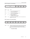
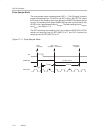
17.2.2 ADC12 Inputs and Multiplexer
The eight external and four internal analog signals are selected as the channel
for conversion by the analog input multiplexer. The input multiplexer is a
break-before-make type to reduce input-to-input noise injection resulting from
channel switching as shown in Figure 17−2. The input multiplexer is also a
T-switch to minimize the coupling between channels. Channels that are not
selected are isolated from the A/D and the intermediate node is connected to
analog ground (AV
SS
) so that the stray capacitance is grounded to help
eliminate crosstalk.
The ADC12 uses the charge redistribution method. When the inputs are
internally switched, the switching action may cause transients on the input
signal. These transients decay and settle before causing errant conversion.
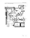
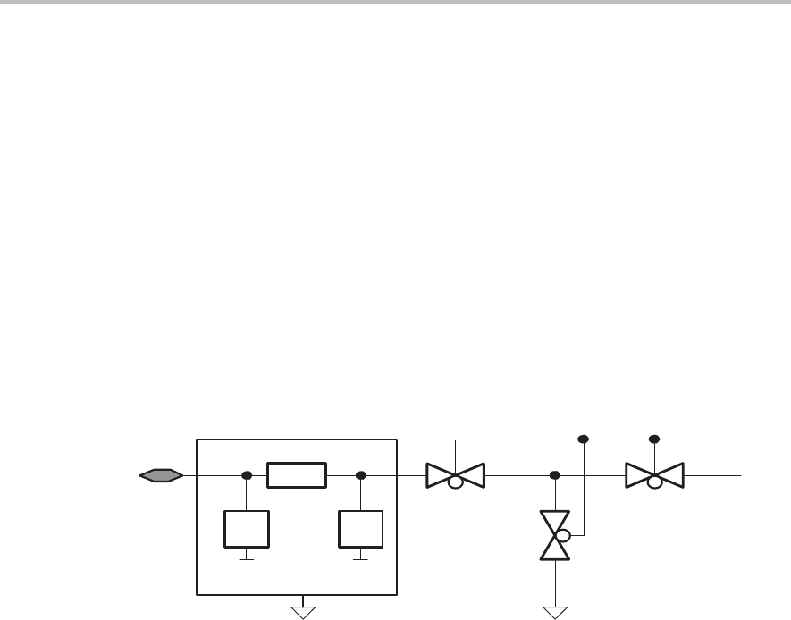
Figure 17−2. Analog Multiplexer
R ~ 100 Ohm
ESD Protection
ADC12MCTLx.0−3
Input
Ax
Analog Port Selection
The ADC12 inputs are multiplexed with the port P6 pins, which are digital
CMOS gates. When analog signals are applied to digital CMOS gates,
parasitic current can flow from V
CC
to GND. This parasitic current occurs if the
input voltage is near the transition level of the gate. Disabling the port pin buffer
eliminates the parasitic current flow and therefore reduces overall current
consumption. The P6SELx bits provide the ability to disable the port pin input
and output buffers.
; P6.0 and P6.1 configured for analog input
BIS.B #3h,&P6SEL ; P6.1 and P6.0 ADC12 function