


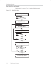


Flash Memory Registers
5-20
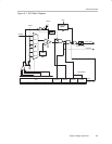
Flash Memory Controller
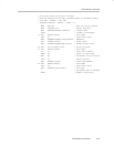
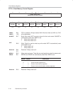
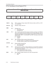
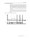
FCTL3, Flash Memory Control Register FCTL3
15 14 13 12 11 10 9 8
FWKEYx, Read as 096h
Must be written as 0A5h
76543210
Reserved Reserved EMEX LOCK WAIT ACCVIFG KEYV BUSY
r0 r0 rw-0 rw-1 r-1 rw−0 rw-(0) r(w)−0
FWKEYx
Bits
15-8
FCTLx password. Always read as 096h. Must be written as 0A5h or a PUC
will be generated.
Reserved
Bits
7-6
Reserved. Always read as 0.
EMEX
Bit 5 Emergency exit
0 No emergency exit
1 Emergency exit
LOCK
Bit 4 Lock. This bit unlocks the flash memory for writing or erasing. The LOCK bit
can be set anytime during a byte/word write or erase operation and the
operation will complete normally. In the block write mode if the LOCK bit is set
while BLKWRT=WAIT=1, then BLKWRT and WAIT are reset and the mode
ends normally.
0 Unlocked
1 Locked
WAIT
Bit 3 Wait. Indicates the flash memory is being written to.
0 The flash memory is not ready for the next byte/word write
1 The flash memory is ready for the next byte/word write
ACCVIFG
Bit 2 Access violation interrupt flag
0 No interrupt pending
1 Interrupt pending
KEYV
Bit 1 Flash security key violation. This bit indicates an incorrect FCTLx password
was written to any flash control register and generates a PUC when set. KEYV
must be reset with software.
0 FCTLx password was written correctly
1 FCTLx password was written incorrectly
BUSY
Bit 0 Busy. This bit indicates the status of the flash timing generator.
0 Not Busy
1 Busy