


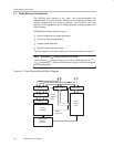
Flash Memory Operation
5-5
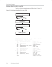
Flash Memory Controller
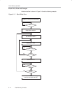
5.3.2 Erasing Flash Memory
The erased level of a flash memory bit is 1. Each bit can be programmed from
1 to 0 individually but to reprogram from 0 to 1 requires an erase cycle. The
smallest amount of flash that can be erased is a segment. There are three
erase modes selected with the ERASE and MERAS bits listed in Table 5−1.
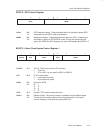
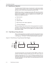
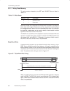
Table 5−1.Erase Modes
MERAS ERASE
Erase Mode
0 1 Segment erase
1 0 Mass erase (all main memory segments)
1
1 Erase all flash memory (main and information segments)
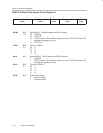
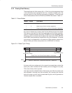
Any erase is initiated by a dummy write into the address range to be erased.
The dummy write starts the flash timing generator and the erase operation.
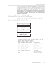
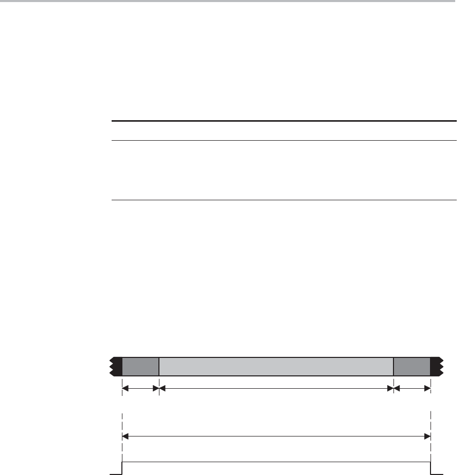
Figure 5−4 shows the erase cycle timing. The BUSY bit is set immediately after
the dummy write and remains set throughout the erase cycle. BUSY, MERAS,
and ERASE are automatically cleared when the cycle completes. The erase
cycle timing is not dependent on the amount of flash memory present on a
device. Erase cycle times are equivalent for all MSP430F1xx devices.
Figure 5−4. Erase Cycle Timing
BUSY
Erase Operation Active
t
All
Erase
= t
Mass
Erase
= 5297/f
FTG
, t
Seg
Erase
= 4819/f
FTG
Erase Time, V
CC
Current Consumption is Increased
Generate
Programming Voltage
Remove
Programming Voltage
A dummy write to an address not in the range to be erased does not start the
erase cycle, does not affect the flash memory, and is not flagged in any way.
This errant dummy write is ignored.
Interrupts should be disabled before a flash erase cycle. After the erase cycle
has completed, interrupts may be re-enabled. Any interrupt that occurred
during the erase cycle will have its associated flag set, and will generate an
interrupt request when re-enabled.