ADC10 Operation
18-17
ADC10
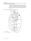
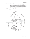
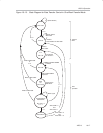
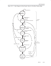
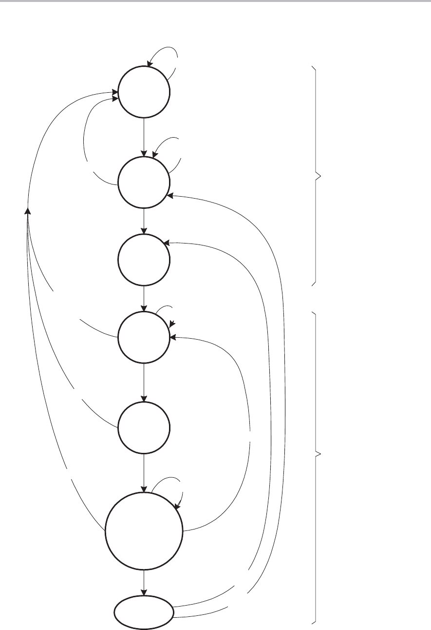
Figure 18−10. State Diagram for Data Transfer Control in One-Block Transfer Mode
DTC idle
DTC reset
n=0 (ADC10DTC1)
Initialize
Start Address in ADC10SA
Wait until ADC10MEM
is written
Wait
for
CPU ready
Write to ADC10MEM
completed
Transfer data to
Address AD
AD = AD + 2
x = x − 1
Synchronize
with MCLK
1 x MCLK cycle
n is latched
in counter ’x’
x > 0
DTC init
Wait for write to
ADC10SA
Write to
ADC10SA
Write to ADC10SA
x = 0
Prepare
DTC
DTC
operation
Write to ADC10SA
or
n = 0
Write to ADC10SA
x = n
AD = SA
n = 0
ADC10IFG=1
ADC10TB = 0
and
ADC10CT = 0
ADC10TB = 0
and
ADC10CT = 1
n ≠ 0


