


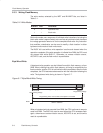

Flash Memory Operation
5-16
Flash Memory Controller
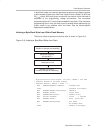
Programming Flash Memory via JTAG
MSP430 devices can be programmed via the JTAG port. The JTAG interface
requires four signals (5 signals on 20- and 28-pin devices), ground and
optionally V
CC
and RST/NMI.
The JTAG port is protected with a fuse. Blowing the fuse completely disables
the JTAG port and is not reversible. Further access to the device via JTAG is
not possible For more details see the Application report Programming a
Flash-Based MSP430 Using the JTAG Interface at www.ti.com/sc/msp430.
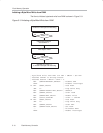
Programming Flash Memory via the Bootstrap loader (BSL)
Every MSP430 flash device contains a bootstrap loader. The BSL enables
users to read or program the flash memory or RAM using a UART serial
interface. Access to the MSP430 flash memory via the BSL is protected by a
256-bit, user-defined password. For more details see the Application report
Features of the MSP430 Bootstrap Loader at www.ti.com/sc/msp430.
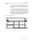
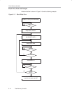
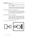
Programming Flash Memory via a Custom Solution
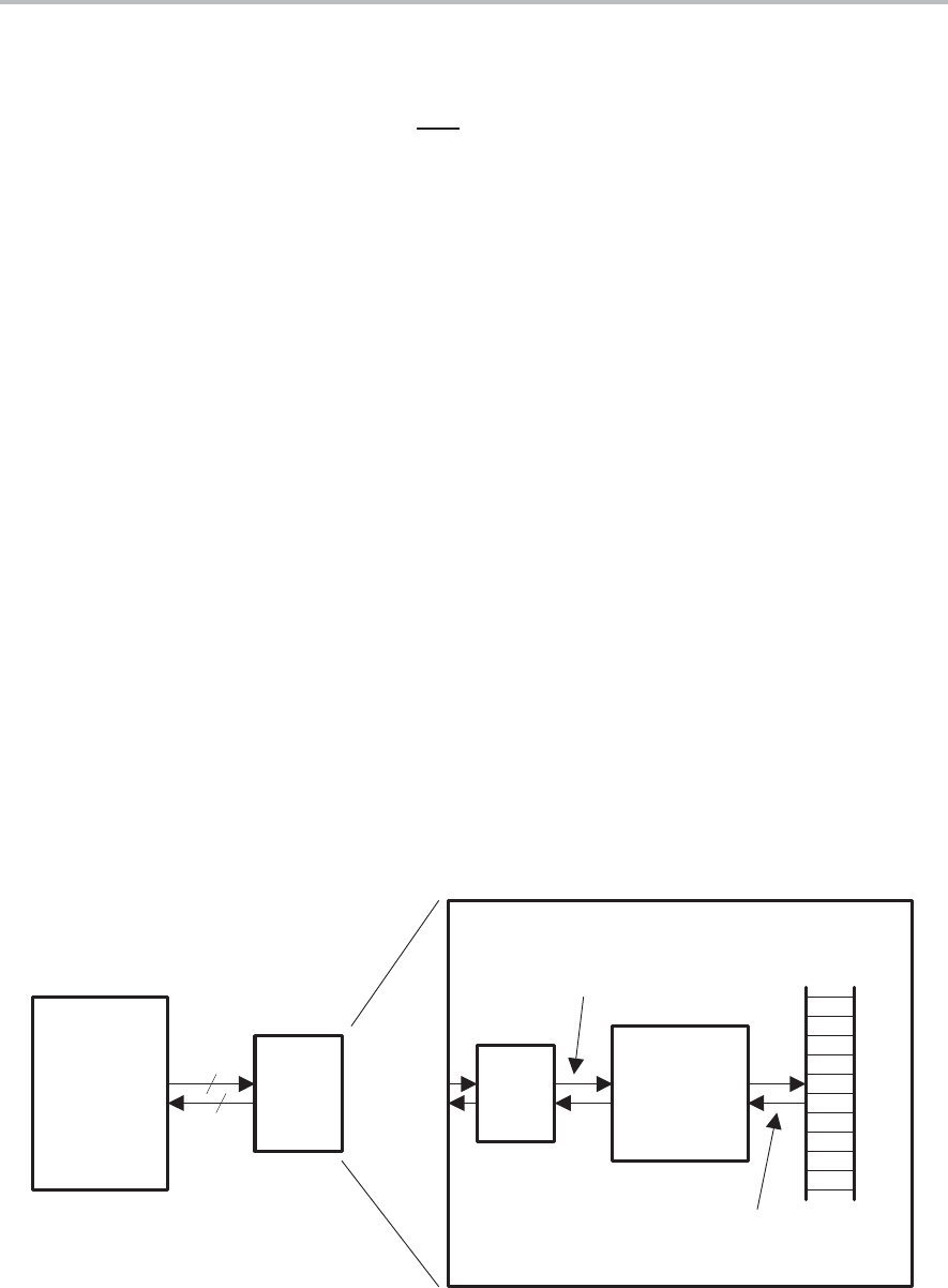
The ability of the MSP430 CPU to write to its own flash memory allows for
in-system and external custom programming solutions as shown in
Figure 5−12. The user can choose to provide data to the MSP430 through any
means available (UART, SPI, etc.). User-developed software can receive the
data and program the flash memory. Since this type of solution is developed
by the user, it can be completely customized to fit the application needs for
programming, erasing, or updating the flash memory.
Figure 5−12. User-Developed Programming Solution
Host
Flash Memory
UART,
Px.x,
SPI,
etc.
CPU executes
user software
Commands, data, etc.
Read/write flash memory
MSP430