


TMP92CM22
2007-02-16
92CM22-98
(2) The cautions at the time of the functional change of a
CSn .
A chip select signal output has the case of a combination terminal with a
general-purpose port function. In this case, an output latch register and a function control
register are initialized by the reset action, and an object terminal is initialized by the port
output (“1” or “0”) by it.
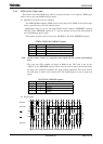
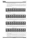
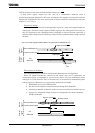
Functional change
Although an object terminal is changed from a port to a chip select signal output by
setting up a function control register (PnFC register), the short pulse for several ns
may be outputted to the changing timing. Although it does not become especially a
problem when using the usual memory, it may become a problem when using a special
memory.
X
X
n+2
Internal address bus
Function control signal
Pxx
n
n+2
A23 to A0
A port is set as
CSn
.
n
Output port
CSn
Internal
Signal
External
Signal
Output pulse
t
AD3
* XX is a function register address.(When an output port is initialized by “0”)
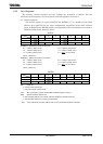
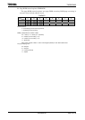
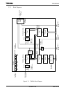
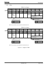
The measure by software
The countermeasures in S/W for avoiding this phenomenon are explained.
Since CS signal decodes the address of the access area and is generated, an
unnecessary pulse is outputted by access to the object CS area immediately after
setting it as a CSn function. Then, if internal area is accessed also immediately after
setting a port as CS function, an unnecessary pulse will not output.
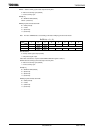
1. Prohibition of use of an NMI function
2. The ban on interruption under functional change (DI command)
3. A dummy command is added in order to carry out continuous internal access.
4. (Access to a functional change register is corresponded by 16-bit command.
(LDW command))
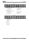
XX+1 n+2
Internal address bus
Function control signal
Pxx
n
n+2
A23 to A0
A port is set as
CSn
.
XX
Output port
CSn
Internal
signal
External
signal
Dummy access