


TMP92CM22
2007-02-16
92CM22-255
7. Points to Note and Restrictions
(1) Notation
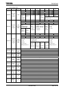
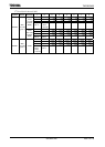
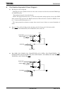
1. The notation for built-in I/O registers is as follows register symbol <Bit symbol>.
Example: TA01RUN<TA0RUN> denotes bit TA0RUN of register TA01RUN.
2. Read-modify-write instructions (RMW)
An instruction in that the CPU reads data from memory and writes the data to the
same memory location by using one instruction.
Example 1: SET 3, (TA01RUN) … Set bit3 of TA01RUN.
Example 2: INC 1, (100H) … Increment the data at 100H.
• Examples of read-modify-write instructions on the TLCS-900
Exchange instruction
EX (mem), R
Arithmetic operations
ADD (mem), R/# ADC (mem), R/#
SUB (mem), R/# SBC (mem), R/#
INC #3, (mem) DEC #3, (mem)
Logic operations
AND (mem), R/# OR (mem), R/#
XOR (mem), R/#
Bit manipulation operations
STCF #3/A, (mem) RES #3, (mem)
SET #3, (mem) CHG #3, (mem)
TSET #3, (mem)
Rotate and shift operations
RLC (mem) RRC (mem)
RL (mem) RR (mem)
SLA (mem) SRA (mem)
SLL (mem) SRL (mem)
RLD (mem) RRD (mem)
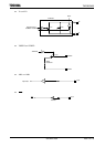
3. f
OSCH
, fc, f
FPH
, f
SYS,
and one state
The clock frequency that is inputted from X1 and X2 is called “f
OSCH
”. The clock that is
selected by PLLCR<FCSEL> register is called “fc”.
The clock that selected by SYSCR1<SYSCK> is called “f
FPH
”. The clock frequency that is
give by “f
FPH
”
divided by 2 is called “f
SYS
”.
One cycle of “f
SYS
” is referred to as one state.