TMP92CM22
2007-02-16
92CM22-228
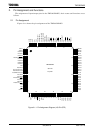
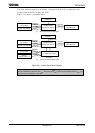
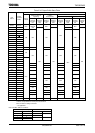
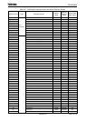
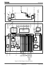
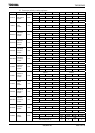
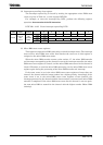
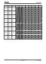
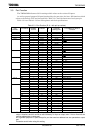
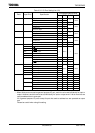
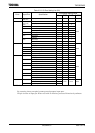
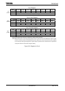
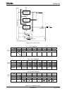
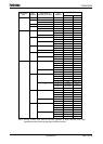
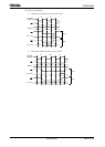
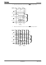
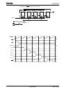
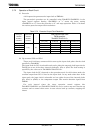
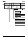
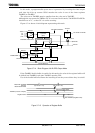
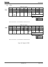
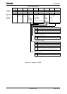
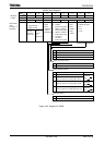
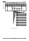
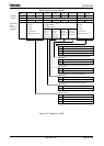
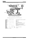
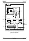
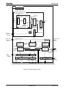
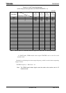
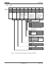
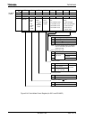
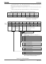
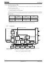
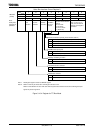
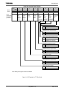
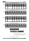
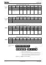
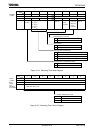
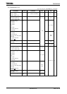
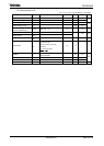
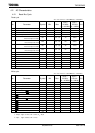
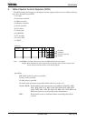
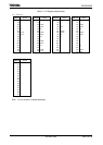
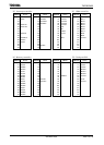
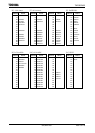
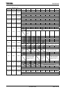
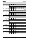
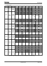
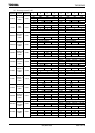
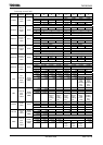
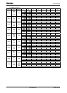
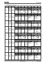
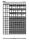
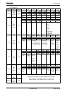
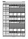
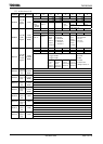
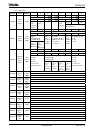
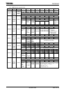
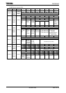
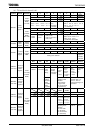
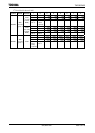
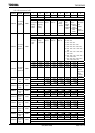
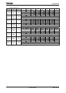
5. Table of Special Function Registers (SFRs)
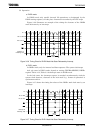
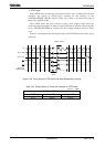
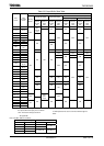
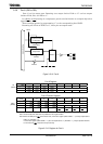
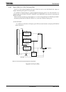
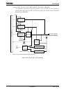
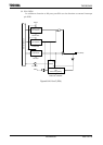
The SFRs include the I/O ports and peripheral control registers allocated to the 8 Kbytes address
space from 000000H to 001FFFH.
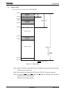
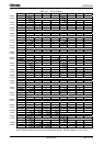
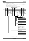
(1) I/O port
(2) Interrupt controller
(3) DMA controller
(4) Memory controller
(5) Clock gear/PLL
(6) 8-bit timer
(7) 16-bit timer
(8) UART/SIO
(9) I
2
C bus/SIO
(10) 10-bit ADC
(11) WDT
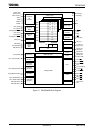
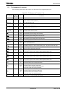
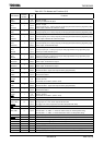
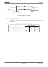
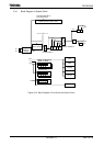
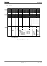
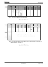
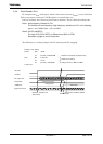
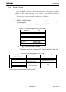
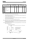
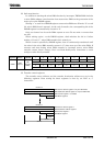
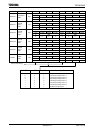
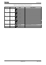
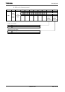
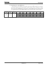
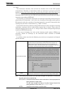
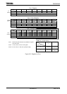
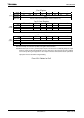
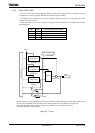
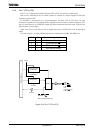
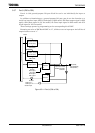
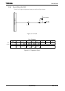
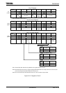
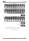
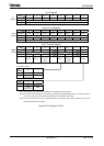
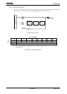
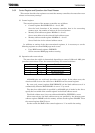
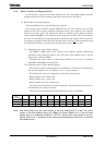
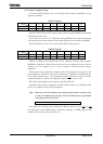
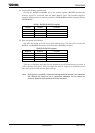
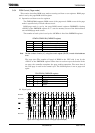
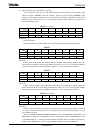
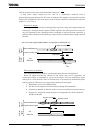
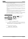
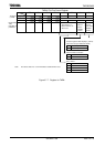
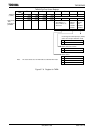
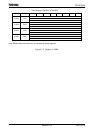
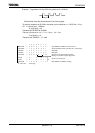
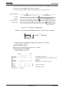
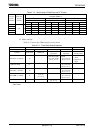
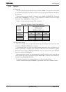
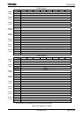
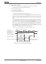
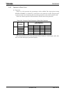
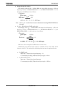
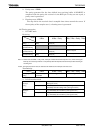
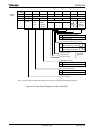
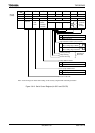
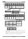
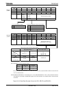
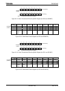
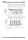
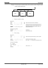
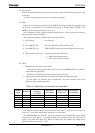
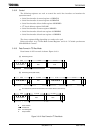
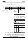
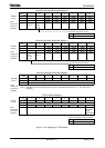
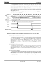
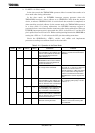
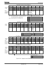
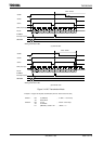
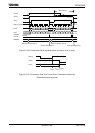
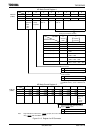
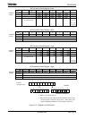
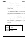
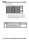
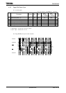
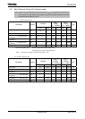
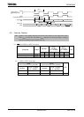
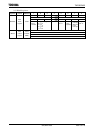
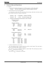
Table layout
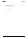
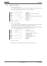
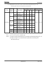
Note: “Prohibit RMW” in the table means that you cannot use RMW instructions on these register.
Example: When setting bit0 only of the register PxCR, the instruction “SET 0, (PxCR)” cannot be used.
The LD (Transfer) instruction must be used to write all eight bits.
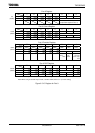
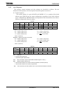
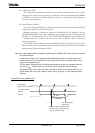
Read/Write
R/W: Both read and write are possible.
R: Only read is possible.
W: Only write is possible.
W*: Both read and write are possible (when this bit is read as 1).
Prohibit RMW: Read-modify-write instructions are prohibited. (The EX, ADD,
ADC, BUS, SBC, INC, DEC, AND, OR, XOR, STCF, RES, SET,
CHG, TSET, RLC, RRC, RL, RR, SLA, SRA, SLL, SRL, RLD, and
RRD instruction are read-modify-write instructions.)
R/W∗: Read-modify-write is prohibited when controlling the pull-up
resistor.
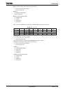
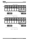
Initial value after reset
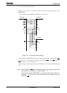
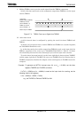
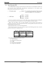
Symbol Address
Name
7 6 1 0
Bit symbol
Read/Write
Remarks